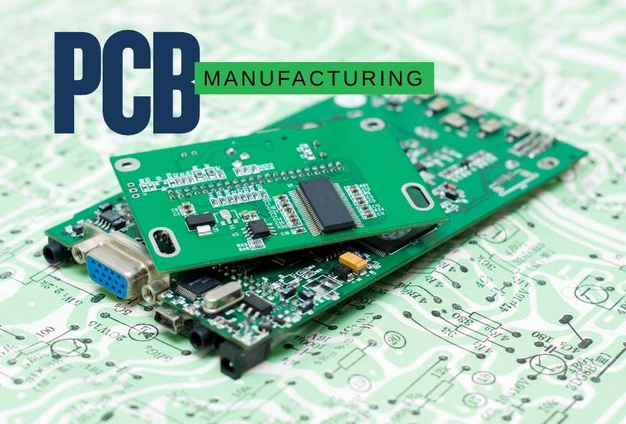
Explore the PCB manufacturing process from design to production and learn how they support modern electronics in devices.
PCB Manufacturing: From Design to Real Product!
Estimated reading time: 4 minutes
Introduction:
Every electronic device – from smartphones to robots – relies on Printed Circuit Boards (PCBs). While students often build circuits on breadboards, real-world products require compact, reliable, and manufacturable PCB designs. This article explains the complete journey of PCB manufacturing, from initial design to final production. This article aims to help students understand how engineering decisions, material selection as well as manufacturing processes transform a simple circuit into a scalable, real-world product.
PCB DESIGN AND MANUFACTURING PROCESS
Printed Circuit Boards (PCBs) are the backbone of modern electronics by not only mechanically supporting but also electrically connecting components. The journey begins with schematic designs, where engineers define how components such as resistors, microcontrollers, and sensors are connected to each others. This is followed by PCB layout, where the circuit is translated into physical copper traces on a board, either restricted or unrestricted by enclosure designs, using software tools such as KiCad or Altium Designer. Sometimes PCBs are designed for already existing Outer Mould design or sometimes as an initial stage for a new product development.
Also Read: Integrating PCBs into Energy Recovery Systems for Sustainable Manufacturing
Engineers must plan PCB layouts carefully to ensure optimal performance. They design wider traces for high-current paths, isolate sensitive signals to block interference and also organize component placement to control noise. Before sending the final Gerber files to manufacturing, engineers apply two critical design checks:
- Design for Manufacturability (DFM): This ensures we can fabricate the board cleanly without production defects.
- Design for Assembly (DFA): This ensures we can solder and mount the components efficiently onto the board.
The PCB manufacturing process involves multiple steps:
- Substrate preparation: The middle part on which the copper is traced usually have two sides complete copper. Typically, FR4 material (fiberglass with copper layers)
- Etching: A light-sensitive photoresist is applied to the copper surface. The PCB pattern is transferred using UV exposure, and unwanted copper is removed through chemical etching to form the required traces.
- Drilling: Creating holes for through-hole components and vias(upper and bottom layer connections).
- Plating: Adding conductive material inside holes
- Solder mask application: Protecting copper and preventing short circuits, usually green is used as an industry standard and visibility of components and cost cutting.
- Silkscreen printing: Adding labels and component markings for assembly.
After fabrication, we assemble components using Surface Mount Technology (SMT) or through-hole soldering. Firstly, automated pick-and-place machines precisely position the components. Then, the board undergoes reflow soldering to lock everything securely in place.
Testing is a crucial stage. During testing, we check boards for defects using methods like Automated Optical Inspection (AOI), functional testing, and flying probe testing. Once the designs are verified in R&D, PCB moves to mass production and product assembly, where design optimization ensures cost efficiency and reliability.
Also Read: Scientists Discovered How CO2 Turns Into Fuel
EDUCATIONAL OPPORTUNITIES in PCB Manufacturing
Students interested in PCB design and manufacturing can pursue degrees in Electronics, Electrical Engineering, or even Mechatronics. To begin with, these programs provide a strong theoretical foundation in circuit design and semiconductor devices. They also equip students with practical knowledge in embedded systems, preparing them directly for hands-on work in the hardware industry.
Hands-on skills are critical in this domain. Students should learn:
- PCB design tools (KiCad, Eagle, Altium)
- Circuit simulation and debugging
- Soldering and prototyping techniques
- Basics of manufacturing processes like etching and photolithography.
Internships in electronics companies expose students to production workflows such as design validation, component sourcing, and manufacturing optimization. Understanding constraints like cost, thermal management, and scalability is essential for transitioning from student projects to industrial products.
Also Read: Understanding LED Types and Their Unique Production Methods – Part II
CAREER PATH
PCB design and manufacturing offer diverse career opportunities. For instance, entry-level roles include PCB Design Engineer, Hardware Engineer, and Embedded Systems Developer. Professionals here work actively on schematic design, layout optimization and also system testing.
With experience, engineers can move into advanced roles such as Product Development Engineer, Electronics Architect, or Manufacturing Specialist. Specialized fields include high-speed PCB design, RF circuits, and power electronics.
Industries such as consumer electronics, automotive, aerospace, and IoT startups actively seek PCB professionals. There are also opportunities in research and development, focusing on advanced manufacturing techniques and miniaturization.
CONCLUSION: PCB design and manufacturing
PCB manufacturing is a crucial step in converting ideas into real-world products. Consequently, students should go beyond breadboard experiments and start designing their own PCBs to understand real engineering challenges. By doing so, they gain practical experience with industry standards. Studying processes like photolithography, assembly, and testing gives us deeper insight into how manufacturers build products.
By combining theoretical knowledge with hands-on experience, students can develop strong problem-solving skills and engineering intuition. Attending workshops, exploring fabrication labs, and building real projects will help transform curiosity into a successful career in electronics and embedded systems. Finally, taking these practical steps turns basic concepts into industry-ready skills.
References:
- Khandelwal, Y. (2024). An In-Depth Analysis of Printed Circuit Board (PCB) manufacturing processes. Figshare.
- Italia, R. (2021). An analysis of printed circuit board (PCB) manufacturing processes. International Journal on Science and Technology.
Reviewed by Dr. Charudatta PathakEdited by Juveriya Khan
- Author
- Latest Posts

Virendra Singh is a Product Development Engineer and Production Head specializing in PCB design, robotics, and AI-enabled hardware systems. With a strong background in electronics and hands-on engineering, he focuses on transforming ideas into manufacturable products, covering the complete cycle from circuit design to production.
He has trained over 1,000 students and 100+ educators in robotics and embedded systems, with an emphasis on practical, real-world learning. His work includes developing modular electronics platforms, IoT systems, and AI-based learning devices aimed at simplifying complex technology for students and innovators.