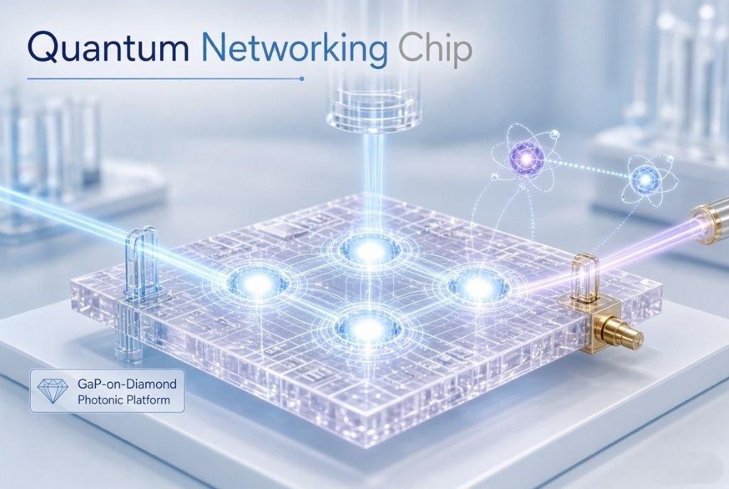
Imagine texting a friend across town and knowing no one can intercept the message, even with the world’s best computers. That kind of security is one goal of quantum networks. Right now, those networks are still hard to build because the tiny quantum bits (qubits) that hold the information don’t easily interact with the light that carries the messages. A team just showed a new way to put the right materials together so photons and diamond-based qubits interact more strongly and reliably. It can be called hybrid GaP-diamond quantum networking. The process can be repeated at high success rates. This brings practical quantum links for banks, hospitals, and power grids a step closer.
Researchers Nicholas S. Yama, Chun-Chi Wu, Fariba Hatami, and Kai-Mei Fu at Washington University and Pacific Northwest National Laboratory created a hybrid platform. They grew gallium phosphide (GaP) nanophotonic cavities directly on a diamond substrate. GaP handles light well and has useful nonlinear properties. Diamond hosts solid-state qubits (specifically silicon-vacancy centers) that can store quantum information. The work appeared in the open-access journal Optica Quantum on 15 October 2026.
They fabricated more than 600 of these cavities with a 99.5 % yield. That high success rate matters because building one perfect device in a lab is not the same as making hundreds that work the same way. The devices reached above-unity cooperativity, meaning the photon-qubit interaction is strong enough to read out the qubit’s spin state reliably through the light. Different spin states produce distinct spectral signatures, so the system can “see” the qubit switch states.
Why hybrid quantum networking matters for everyday life and jobs
Quantum networks could protect medical records, financial transactions, and power-grid control signals far better than today’s encryption. Companies that build and operate that hybrid quantum networking equipment will need people who understand photonics, materials science, and quantum engineering.
Teens who enjoy both physics and hands-on building can explore branches of engineering like electrical engineering, materials science, or applied physics. Internships at national labs or quantum startups often start with clean-room work, optical alignment, or simple device testing. Skills in coding (Python is common) and basic data analysis help even in experimental groups.
The same platform may later support quantum sensors or small-scale quantum processors. Early familiarity with these hybrid material systems helps students better decide which courses and projects to prioritize.
Reference
Yama, N. S., Wu, C.-C., Hatami, F., & Fu, K.-M. C. (2026). Efficient spin-photon interactions in a scalable nanophotonic platform. Optica Quantum, 4(4), 511–517. https://doi.org/10.1364/OPTICAQ.607235
Charudatta Pathak was a student at St. Aloysius High School in Bhusawal, established in 1874, making it one of India's oldest convent institutions. He earned his bachelor's degree in mechanical engineering from SSVPS College of Engineering, Dhule in 1995, demonstrating exceptional academic achievement. Thereafter, he launched his career as a CNC programmer in a toolroom. He has utilized FANUC, Deckel, Maho, and Mikron controllers to operate 2-axis and 3-axis machines for the fabrication of jigs, fixtures, dies, and molds. He commenced his career as an academic in 1996, when he assumed the role of lecturer at SSVPS College of Engineering, Dhule. Additionally, he earned his post-graduate degree in CAD/CAM from L. D. College of Engineering, Ahmedabad, in 2000, and then acquired a Ph.D. from COEP in 2011 while concurrently engaged in teaching. Until 2023, he occupied many academic roles, including lecturer, assistant professor, professor, dean, principal, director, and vice chancellor at both public and private universities throughout India. From 2008 to 2010, he served as the project lead in the CAE department of a European multinational firm. During his 28-year professional tenure, he identified a need for dependable books targeted at students in grades 8 to 12, particularly for nascent career planning. He founded ENTECH Digital Magazine, a free monthly publication available on entechonline.com and magzter.com. Teens with a strong interest in Science, Technology, Engineering, and Mathematics (STEM) who aspire to pursue careers in these fields may find ENTECH Digital Magazine beneficial.
Dinesh Joshi is a leading consultant in the field of product design and development, production engineering, industrial engineering, and program management. He has worked with esteemed domestic as well as European and US organizations.
Mr. Dinesh G. Joshi has completed Graduation in Mechanical Engineering from Pune University and thereafter pursued Post Graduation in Production Engineering from Walchand College of Engineering Sangli (Shivaji University). He is member of Project Management Institute (PMI), Pennsylvania, USA as well as Indian Institute of Welding (IIW) Kolkata. He has good blend of diversified experience of about 22 years in Product Design and Development, Production Engineering, Industrial Engineering and Program Management by virtue of working in the esteemed domestic as well as European and US organizations in addition to 5 years of academic experience.