Every video call you make travels as pulses of light through glass fibers. In fact, those fibers work because glass loses very little light over distance. Quantum computers built from light need the same trick, but on a tiny chip. Now, a research team has built low-loss quantum photonic chips for visible light. These chips steer light with small squeezes instead of heat. Mayank Mishra led the work at the University of Arizona’s Wyant College of Optical Sciences. Partners at Sandia National Laboratories and the University of Colorado Boulder joined him. Their best waveguide loses only about 2.6 decibels of light per meter at 780 nanometers. The team reported the results on October 27, 2026, in Nature Communications (DOI: 10.1038/s41467-026-77969-0). As a result, deeper and more reliable quantum light circuits now look far more practical.
The Science Explained: How Quantum Photonic Chips Steer Light
Waveguides and Interferometers in Plain Words
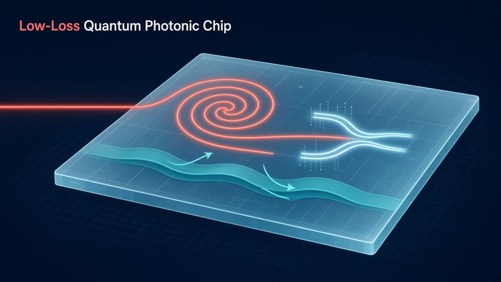
A photonic chip moves light the way a circuit board moves electric current. Instead of copper wires, it uses waveguides, thin stripes of glassy material that trap light. In this study, the silicon nitride core measures 50 nanometers by 3.6 micrometers. A thick blanket of silicon dioxide, 12.5 micrometers deep, surrounds that core. Because of this thin core, much of the light travels in the glass. Engineers call this a low-confinement design, and it scatters very little light. To steer light, the chip uses a Mach-Zehnder interferometer, or MZI. First, the MZI splits light into two paths. Then it lets the two beams meet again. If one path slows its light slightly, the beams add up or cancel out. In other words, a tiny delay decides where the light exits. Many linked MZIs form a programmable processor, following a layout proposed by Clements and colleagues.
Strain Instead of Heat
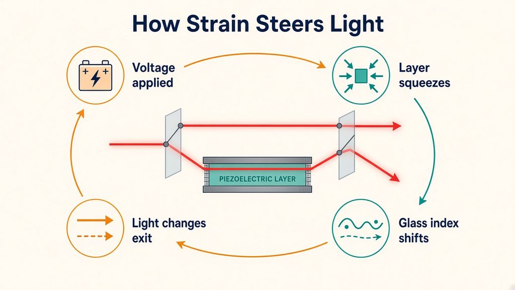
Most chips shift that delay by warming one path with a small heater. Heat changes how fast light moves, but it spreads and wastes power. This team chose a different tool, a piezoelectric actuator. Such a material flexes when it feels a voltage. Here, a 0.46-micrometer layer of aluminum nitride sits between two aluminum electrodes. The actuator lies about three micrometers below the light-carrying core. When voltage arrives, the layer strains the glass around the waveguide. That strain changes the refractive index, which sets the speed of light inside the glass. As a result, the light in that arm gains or loses a little phase.
According to the team, silicon dioxide drives most of this change. Silicon nitride, in contrast to that, pushes the index slightly the other way. Because squeezing needs almost no steady current, the actuator stays cool. In 2019, Eichenfield and Leenheer tested an earlier version of this idea for cryogenic use.
Fig. 1: Explainer Illustration
Challenges and Motivation Behind Low-Loss Photonic Chips
The Visible-Light Knowledge Gap
Many of the best quantum light tools work with visible or near-visible light. Single-photon sources and quantum memories, for example, naturally operate in this range. Rubidium atoms, strontium atoms and some quantum dots also pair well with these wavelengths. However, tightly confined visible waveguides scatter a lot of light. On the other hand, quantum circuits must pass light through many steps without losing photons. Each lost photon can spoil a delicate quantum calculation. In particular, earlier piezo-tuned visible chips lost 35 to 100 decibels per meter. As a result, they could not support the deep circuits that scalable quantum computing needs. Low-confinement silicon nitride already offered loss below 1 decibel per meter at visible wavelengths. Yet aluminum nitride actuators had appeared only with tightly confined waveguides. That missing pairing formed the main knowledge gap. Research on chip-based quantum memory shows why clean photon storage and routing matter so much.
Heat, Hysteresis and Foundry Limits
Two older options each carried a serious drawback. First, heater-based thermo-optic switches run slowly and burn steady power. Their heat also leaks into nearby paths, which engineers call crosstalk. Second, lead zirconate titanate, or PZT, switches faster with less crosstalk. Unfortunately, PZT shows strong hysteresis, so its response depends on its past voltage. It also does not fit standard chip-factory processes, known as CMOS. Aluminum nitride actuators avoid both problems. In fact, Sandia National Laboratories describes related devices from its CMOS foundry. But the thick glass cladding of low-loss waveguides creates a new hurdle. Thick glass makes the structure stiff, so squeezing it becomes harder.
To fix this, the team carved an extended undercut beneath the actuator. This gap lets the actuator flex and focus stress near the light. As a result of this design, the chip kept a strong response despite thick cladding. Their motivation stayed simple: build quantum circuits that scale without drowning in loss.
Key Findings on Low-Loss Quantum Photonic Chips
Measured Loss in the Quantum Photonic Chip
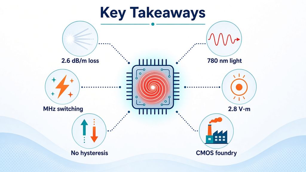
The paper highlights propagation loss, the light lost along each meter. To measure it, the team photographed faint light scattering from a 1.8-meter spiral waveguide. Brighter spots mean more light still remains inside the guide at that point. A straight-line fit of the brightness gave a loss of 2.57 decibels per meter. Next, a second method called optical frequency-domain reflectometry checked the result. It found about 2.96 decibels per meter in the gently curved sections. Across all tests, waveguides without actuators stayed at or below 3 decibels per meter. Waveguides with actuators lost more, about 7.2 to 8.3 decibels per meter. Even so, that beats about 38 decibels per meter in a tightly confined chip. Tiny metal bumps poking into the glass caused most of that extra loss. Direct metal absorption, by contrast, added only about 0.05 decibels per meter. Overall, each 8.7-centimeter phase shifter lost just 0.63 decibels.
Speed, Voltage and Holding Power
Speed matters because quantum circuits must reconfigure quickly between tasks. A network analyzer test showed the response dropping by half near 7 megahertz. In addition, a 1-megahertz square wave gave a fall time near 50 nanoseconds. Both tests agreed, so the bandwidth value looks solid. To flip the light fully, the 8.7-centimeter spiral needed about 32.5 volts. That gives a voltage-length product of 2.8 volt-meters at 780 nanometers. Lower numbers mean a more efficient switch. Voltage sweeps from minus 10 to 120 volts and back traced nearly identical curves. In other words, the device showed negligible hysteresis. Holding a setting cost less than one nanowatt at 5 volts and room temperature. The team also merged loss and voltage into one score, the voltage-loss product. Their chip reached about 20.2 volt-decibels on this score. By comparison, a tightly confined rival using the same strain effect scored about 50.7 volt-decibels.
Why Lower Loss Multiplies Success
Small loss savings grow huge inside large quantum circuits. To show this, the team simulated circuits that create entangled photon states. A Bell state links two photons, while a GHZ state links several at once. At a 20-volt drive, today’s chip loses about 1 decibel per phase shifter. A future design could cut that to about 0.2 decibels. As a result, Bell-state success rises by roughly 100 times. Even more striking, four-mode GHZ success rises by more than 100 million times. Because each photon passes many phase shifters, losses multiply along the way.
So, in a deep circuit, a fraction of a decibel decides success or failure. The researchers also outlined how to reach that target. Freeing selected spiral sections to flex could lower the voltage-loss product five to ten times. Moving the actuator farther from the core could also trim the extra metal loss. Together, these steps might push the product down to about 0.7 to 2 volt-decibels.
Implications: Business, Careers and What to Study
Business Opportunities for Low-Loss Photonic Chips
The foundry angle may matter most for industry. For fabrication, the team used an anneal-free, low-temperature deposition process. That choice lets metal wiring sit safely beneath the waveguide inside one chip. Because of this CMOS fit, chip factories could offer these circuits to quantum companies. The paper lists target uses such as quantum routers and photonic logic circuits. It also names on-chip quantum memories and tunable optical delay lines. Startups building optical quantum computers need exactly this kind of programmable, low-loss hardware. In the same way, firms developing quantum networks need clean routing of single photons. Notably, the U.S. Department of Energy funded the work through its Quantum Systems Accelerator. Over time, single-photon sources, modulators and control electronics could share one integrated chip. That integration would cut size, cost and assembly steps for quantum products. For chip foundries, visible-light quantum circuits could become a fresh product line.
Career Paths, Study Options and Next Steps
This project shows how many skills one chip needs. Mishra designed the layouts and ran simulations. Colleagues at Sandia coordinated fabrication, while others measured and analyzed the devices. Students who enjoy physics and math could aim for careers as photonics engineers. Quantum hardware engineers, semiconductor process engineers and optical test engineers also fit this field. For example, students can study electrical engineering with a photonics focus. Physics programs in optics and quantum mechanics build the core theory. Optical sciences degrees, such as those at the Wyant College, combine both worlds. Materials science and nanofabrication courses teach how to build these thin layers. At the same time, coding skills help with simulations like those in this paper. As for next steps, the team proposed a revised spiral design with freed sections. That design targets loss near 0.2 decibels per phase shifter. If they reach it, eight-mode programmable circuits could generate complex entangled states far more reliably.
Conclusion: A Clearer Path for Quantum Light Chips
This study joins two strengths that rarely appeared together before. On the one hand, low-confinement silicon nitride keeps loss near 2.6 decibels per meter. That figure sets a benchmark for anneal-free silicon nitride with these actuators. On the other hand, aluminum nitride actuators switch light at megahertz speeds. They also need almost no holding power. As a result, the phase shifters lost only 0.63 decibels each. Not only did hysteresis stay negligible, but the process also suits CMOS foundries. Of course, the actuator still adds extra loss, and the team plans design fixes. Even so, the roadmap points toward phase shifters below 0.2 decibels. That level could raise entangled-state success by many orders of magnitude.
For students, the message reaches beyond quantum physics. Low-loss quantum photonic chips need optics, materials, electronics and software experts working together. Anyone curious can start with the open-access Nature Communications paper and its clear figures. Here, careful engineering of glass, metal and strain made the key difference.
References: low-loss quantum photonic chips
Clements, W. R., Humphreys, P. C., Metcalf, B. J., Kolthammer, W. S., & Walmsley, I. A. (2016). Optimal design for universal multiport interferometers. Optica, 3(12), 1460–1465. https://doi.org/10.1364/OPTICA.3.001460
Mishra, M., Choi, G., He, W., Talcott, G. M., Kearney, K., Gehl, M., Leenheer, A., Dominguez, D., Otterstrom, N. T., & Eichenfield, M. (2026). Ultra-low loss piezo-optomechanical low-confinement silicon nitride platform for visible wavelength quantum photonic circuits. Nature Communications. Advance online publication. https://doi.org/10.1038/s41467-026-77969-0
Stanfield, P. R., Leenheer, A. J., Michael, C. P., Sims, R., & Eichenfield, M. (2019). CMOS-compatible, piezo-optomechanically tunable photonics for visible wavelengths and cryogenic temperatures. Optics Express, 27(20), 28588–28605. https://doi.org/10.1364/OE.27.028588
As a seasoned professional, I bring a rich background in strategic planning, institutional effectiveness, and quality assurance to the table. My track record is marked by a proven ability to spearhead the development and implementation of strategic objectives, always with an eye on continuous improvement. I possess deep expertise in managing comprehensive cycles of planning, assessment, analysis, and enhancement of various processes, programs, and services. My adeptness at ensuring adherence to accreditation standards and government regulations is a cornerstone of my professional ethos. My contributions to research have been recognized with an award from the Union Ministry of Energy's Department of Power, underscoring my commitment to excellence and innovation in my field.