Robots, drones and self-driving cars all depend on cameras to understand the world. Yet most cameras still use flat sensors and stacks of correcting lenses. Animal eyes work differently, because their light-sensing retina is curved like a bowl. In fact, a Hong Kong University of Science and Technology team has copied that shape. According to an official HKUST news release, its bionic eye packs 367,500 colour pixels. The curved device also spots motion by itself, sending far less data. In addition, it sees sharply across a field of view wider than 160 degrees. As a result, it could lead to smaller, more efficient eyes for future robots. Still, it remains a research prototype rather than a finished product.
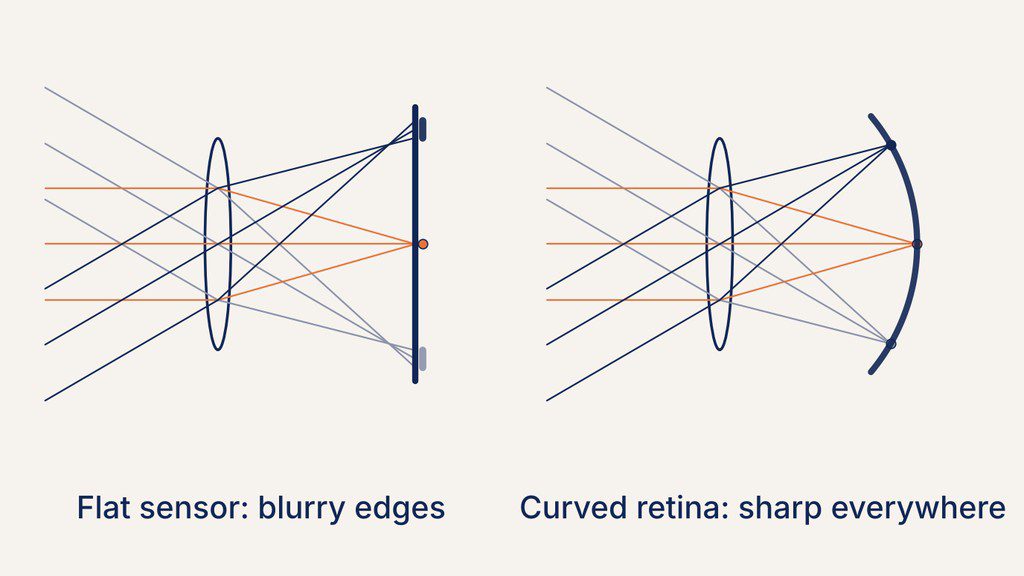
A normal camera focuses light onto a flat chip covered in pixels. However, a simple lens does not focus evenly onto a flat surface. Because of this, the edges of a wide image tend to blur or bend. Engineers call these unwanted errors optical aberrations in the lens system. To fix them, cameras therefore add several extra lenses and outside processing. For that reason, wide-angle cameras often become larger, heavier and more power-hungry. By comparison, the curved retina of an eye matches the way lenses naturally focus. In other words, a bionic eye could see widely with far simpler optics. That is why the HKUST engineers set out to build one.
Explainer: How a Curved Image Sensor Helps
A curved image sensor places its pixels on a dome instead of a flat plate. For example, light from the edge of a scene then lands at a better distance. Each part of the image therefore stays sharper without heavy correction. The HKUST release says such sensors can support compact, wide-angle imaging systems. However, making dense pixels on a strongly curved surface is very hard. After all, standard chipmaking tools, called lithography, mainly suit flat silicon wafers. On a dome, those tools cannot print fine patterns evenly across the surface. So far, this problem has limited the resolution of curved sensors.
Printing Pixels on a Dome With Lasers
To solve this, Professor Fan Zhiyong’s team developed a 3D laser fabrication method. Specifically, the laser writes dense arrays of light-sensitive pixels directly onto a hemisphere. In this way, the team avoided the limits of flat chipmaking tools. The resulting artificial retina reaches 1,905 pixels per inch across its curved surface. In total, it holds 367,500 pixels, close to 400,000. Fan leads the university’s State Key Laboratory of Displays and Opto-Electronics. Indeed, his team works across electronic, computer, chemical and biological engineering. The work appears in the journal Nature Materials, published online on August 17, 2026. Moreover, Professor Zi Yunlong of HKUST (Guangzhou) also contributed to the study.
Fig. 1: A Dome-Shaped Retina Keeps a Wide Scene in Focus
From 100 Pixels to Nearly 400,000
This is not the team’s first attempt at an artificial eye. In 2020, its first-generation device had only 100 sensing pixels. By comparison, the new design holds about 3,675 times as many pixels. Fan says the laser process made that huge jump in pixel count possible. Even so, nearly 400,000 pixels is still small compared with phone cameras. For instance, many smartphone sensors hold tens of millions of pixels on flat chips. With this in mind, the team now aims for more than one million pixels. Fan believes such a device could open uses in robotics and autonomous driving. Each step up in pixels brings the bionic eye closer to real products.
Three Colour Layers Borrowed From Fish
The design draws inspiration from cyprinid fish, the family that includes carp. These fish see in three colours and are good at sensing movement. Similarly, the HKUST retina stacks blue-, green- and red-sensitive layers on each other. Hence, engineers call this stacked arrangement a tandem design. Together, the layers respond to light from 300 to 800 nanometres in wavelength. That range stretches beyond visible light into parts of the ultraviolet and near-infrared. Consequently, the device produces full-colour images from a single curved chip. In this way, nature again provides a useful engineering blueprint.
Wide-Angle Vision Without Extra Lenses
The bionic eye also keeps images sharp across a very wide view. Its aberration-corrected field of view exceeds 160 degrees, according to HKUST. That is close to half a full circle, seen in a single glance. In addition, the curved shape reduces the need for multiple correcting lenses. Equally important, the university says this approach can make vision systems more compact. Smaller, lighter cameras matter greatly for drones and small robots. Meanwhile, a wide view helps machines notice objects approaching from the side. Taken together, these features suit machines that must watch their surroundings constantly. Our story on measuring steel slabs with cameras shows another vision use.
Event-Driven Motion Detection Inside the Sensor
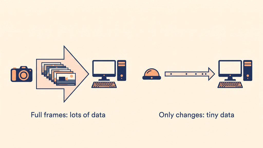
Normal video works by capturing complete images many times every second. A computer then compares those frames to work out what has moved. However, sending every full frame uses a lot of bandwidth and power. The HKUST tandem design instead allows event-driven motion detection inside the sensor. In other words, the chip reports changes rather than whole repeated images. As a result, it no longer needs to send full image sequences for these tasks. Under the study’s test conditions, bandwidth demand fell by more than 99.95%. At the same time, motion recognition reached an accuracy of 98.6%. That comparison was made against ordinary frame-based imaging.
Fig. 2: Sending Only the Changes Cuts Data by More Than 99.95%
Sending Far Less Data
To illustrate the saving, imagine a camera sending 10,000 units of data. With a 99.95% cut, the same task would need only about five units. Less data could mean smaller wireless links, cheaper chips and longer battery life. For example, a delivery drone could react faster while saving energy. Similarly, self-driving cars could spend less computing power on simple motion checks. This idea resembles neuromorphic, or brain-inspired, hardware that processes information near the sensor. Our article on a brain-inspired computer that solves equations explains that wider field. Still, the 99.95% figure applies only to the study’s test conditions. After all, real roads and factories may produce messier, busier scenes.
Business Opportunities for the Bionic Eye
Right now, sensor researchers can study 3D laser fabrication for curved pixel arrays. Within five years, compact wide-angle sensors could be tested in robots and drones. Inspection systems in factories might also use such sensors to spot moving defects. Accordingly, that work could grow demand for optoelectronic engineers and sensor integrators. In the long run, a million-pixel bionic eye could support autonomous vehicles. It might also help edge-AI cameras that process data on the device itself. Consequently, some camera-processing work could move from computers into the sensor. Of course, all of this depends on cost, durability and mass production.
Careers and What to Study
A bionic eye brings together optics, chips, materials and artificial intelligence. To begin with, optoelectronic engineers design pixels that turn light into electrical signals. Process engineers, in turn, develop new fabrication methods like the 3D laser approach. Meanwhile, machine-vision engineers teach robots to understand what their sensors detect. In the US, electrical and electronics engineers earned a median $125,040 in May 2025. Those are figures from the US Bureau of Labor Statistics. The agency projects 8% growth in these jobs through 2035. Pay, however, varies widely between countries and employers. For study, consider electrical engineering, materials science, physics or computer engineering. Optics and photonics courses are especially useful for sensor design.
Limits Worth Keeping in Mind
Note that this device is still a laboratory research prototype. The bandwidth and accuracy figures come only from the study’s test conditions. Moreover, the Nature Materials paper is not open access. For that reason, ENTECH relied on HKUST’s release and did not check the data. Resolution, while far higher than before, remains well below flat phone sensors. Likewise, the release reports no manufacturing cost or long-term durability. Future versions must also prove themselves outside controlled laboratory tests. Even so, printing dense pixels on a dome is a clear engineering advance. In short, the bionic eye shows how copying nature can rethink the camera.
References
The Hong Kong University of Science and Technology. (2026, November 13). HKUST develops high-resolution bionic eye: Integrating full-color wide-angle vision with event-driven motion detection. HKUST News. https://hkust.edu.hk/news/hkust-develops-high-resolution-bionic-eye
Long, Z., Wang, K., He, S., Sun, X., Ye, Z., Li, J., Shen, K., Qiu, X., Ding, Y., Xue, F., Zhou, Y., Kumar, S., Poddar, S., Tan, X., Zi, Y., & Fan, Z. (2026). An aberration-corrected bionic eye for full-colour vision and event-driven motion detection. Nature Materials, 25, 1855-1863. DOI 10.1038/s41563-026-02685-5 (subscription article; cited, not linked).
The article explains aberrations, curved sensors and in-sensor motion detection in clear, student-friendly terms. Its figures match the HKUST release, including 367,500 pixels at 1,905 ppi, a field of view over 160 degrees and a bandwidth cut above 99.95%. It states that ENTECH could not check the subscription paper, and it cites the paper without a link. Readers who want the full methods should consult the original research paper behind this story.
Editorial note
ENTECH is running this Innovation because machine vision is central to robots and self-driving systems, and HKUST shows a working prototype that rethinks the camera itself. The team borrowed the curved retina and motion sensing of animal eyes. Students can see how materials science, chip fabrication, optics and AI connect. It is a research prototype, its figures come from test conditions, and the paper is closed access. For the full details, we suggest readers turn to the original HKUST announcement.
As a seasoned professional, I bring a rich background in strategic planning, institutional effectiveness, and quality assurance to the table. My track record is marked by a proven ability to spearhead the development and implementation of strategic objectives, always with an eye on continuous improvement. I possess deep expertise in managing comprehensive cycles of planning, assessment, analysis, and enhancement of various processes, programs, and services. My adeptness at ensuring adherence to accreditation standards and government regulations is a cornerstone of my professional ethos. My contributions to research have been recognized with an award from the Union Ministry of Energy's Department of Power, underscoring my commitment to excellence and innovation in my field.