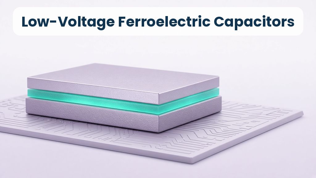
Every time you open an app, your phone pulls data into its working memory. That memory, called DRAM, stores each bit as charge in a tiny capacitor. As chips shrink, however, those capacitors struggle to hold enough charge. Now, a Korean team reports low-voltage ferroelectric capacitors that could help. Their 5-nanometer film switches fully at just 0.6 volts. In addition, it showed no hard breakdown through one trillion switching cycles. Geun Hyeong Park at Seoul National University is the first author. Min Hyuk Park of Seoul National University co-led the study with two Hanyang University researchers. Those two are Daewoong Kwon and Ho Jun Kim. Together, the group spans six Korean institutions and companies. Samsung Electronics scientists and Pohang Accelerator Laboratory staff also took part. The team published the work in Nature Communications on October 29, 2026. Its DOI is 10.1038/s41467-026-78705-4 (Park et al., 2026).
Why Memory Chips Need Low-Voltage Ferroelectric Capacitors
Phones, laptops, and data centers all rely on DRAM for fast working memory. Each memory cell pairs one transistor with one capacitor. The transistor acts like a gate, while the capacitor holds charge like a bucket. A full bucket means one, and an empty bucket means zero. Over time, though, the charge leaks away, so chips must refresh it constantly. As cells shrink, each bucket also gets smaller and holds less charge. For this reason, engineers keep searching for materials that pack more charge into less space.
One promising option is a ferroelectric called hafnium zirconium oxide, or HZO. Its atoms can flip between two stable positions, much like a light switch. Because of this flip, HZO releases five to ten times more charge than usual films. Engineers, as a result, see HZO as a strong candidate for denser memory. Our guide to semiconductors in electronics explains the basic building blocks behind these chips.
Two Roadblocks for Low-Voltage Ferroelectric Capacitors
Still, HZO has two big problems that block its use in memory. First, chips need very fast switching, below 10 nanoseconds for DRAM. Higher voltages give faster switching, but they also wear the film out sooner. Engineers call this tradeoff the speed–endurance dilemma. Second, a scaling rule called the Kay–Dunn law works against thin films. According to this rule, thinner films need a stronger electric field to flip. In other words, thinner films do not lower the switching voltage as hoped. As a result, ultrathin HZO often needs more than one volt to switch fully. Modern chips, by contrast, run on very low voltages to save power. The paper says it resolves both problems, but that word needs care. In fact, the team eases the practical penalty rather than breaking the law itself. Even so, easing it would matter a lot for chip designers.
The Science Explained: A Better Electrode Under a Thin Film
A capacitor works like a sandwich, with a thin film between two metal plates. Here, the plates are titanium nitride, and the filling is 5-nanometer HZO. The team grew the bottom plate atom by atom with plasma at 250 °C. Next, they compared two gas mixes for that plasma step. Ammonia and argon gave crystals that lined up in one tidy direction, called (111). In contrast, nitrogen and argon gave a different, less helpful direction, called (002). The ammonia-grown surface also carried extra nitrogen, which resisted oxidation. As a result, the unwanted oxide layer shrank to about 0.5 nanometers. On top of that, resistance stayed even across a 6-inch wafer, varying under 1%. Think of it as a clean, flat floor for building tiles. Even the electrical resistance dropped slightly on the ammonia-grown plate. A smoother start, in turn, lets the ferroelectric film form better crystals.
Fig. 1: How a Better Electrode Enables Low-Voltage Switching
Switching at 0.6 Volts
That better floor changed how the film switched. On the improved electrode, the 5-nanometer HZO switched fully at just 0.6 volts. At that voltage, it stored a switchable charge of 31.5 microcoulombs per square centimeter. For comparison, the film on the other electrode needed 1.2 volts for less charge. The coercive field, or the push needed to flip atoms, measured 0.62 megavolts per centimeter. That value sat below the usual Kay–Dunn trend for films this thin. The authors link this result to better charge screening at the cleaner interface. In plain terms, the electrode helps cancel stray charges, so atoms flip more easily. Similarly, switching voltages varied less from device to device on the better electrode. Such low spread matters, because of the billions of capacitors in real chips. Reliable chips need nearly identical cells. Earlier ENTECH coverage of magnetic memory chips shows how other teams chase similar goals.
What the Low-Voltage Ferroelectric Capacitors Achieved
Next, the team tested how long the capacitors could keep switching. Endurance matters, because memory cells flip constantly during normal use. The films showed no hard breakdown through one trillion switching cycles. That number came from direct lab measurements at 8.33 million cycles per second. However, the stored charge did fade somewhat during that long test. At 0.6 volts, the charge loss passed a 20% limit after about 600 billion cycles. By one trillion cycles, the loss reached 26.5%. At 1.0 volt, by contrast, the loss stayed lower, at 18.5%. The team also measured switching speed on larger test capacitors. For instance, half the atoms flipped within 42 nanoseconds at 0.6 volts. At 1.0 volt, that time dropped to 8.1 nanoseconds. A small array of 15 capacitors also behaved very evenly. In addition, its stored charge varied by only about 2% across the cells.
Fig. 2: Key Takeaways From the Sub-Volt Capacitor Study
Extrapolated and Simulated Results
Some headline numbers, though, did not come from direct measurement. First, the team extrapolated switching speed to tiny DRAM-sized capacitors about 250 nanometers wide. That estimate suggests sub-nanosecond to low-nanosecond switching, but nobody built those tiny devices yet. Second, the team ran computer simulations of a memory design called common-plate FeRAM. Unlike DRAM, this design keeps data through the ferroelectric state itself. That stored state survives even after the cell’s ordinary charge leaks away. At 1.1 volts, the simulation gave a strong sensing margin of 482 millivolts. Even after long stand-by times, a margin of 201 millivolts remained. In the same simulation, a regular DRAM cell’s margin fell to zero. The model also showed that more stored charge shrinks the capacitor area needed. For example, stronger films could fit a 200-millivolt margin into much smaller cells. Still, these remain simulated results, so real chips must confirm them.
Honest Limits of Low-Voltage Ferroelectric Capacitors
Every early study has limits, and the paper (Park et al., 2026) lists them. Good science, after all, states its boundaries openly. For one, the speed claim rests on extrapolation, not on tiny working devices. Also, the memory margins come from circuit simulations, not a finished chip. The charge fatigue of 26.5% at 0.6 volts also needs improvement. On top of that, the disturbance test ran without access transistors, which real chips need. In addition, the team’s field maps are not lifetime predictions.
The authors also avoid claiming that their design beats every plate-line memory design. Instead, they describe a path from materials to circuits for thin ferroelectric films. Those careful boundaries make the work easier to trust. As a result, readers can separate measured facts from promising projections. Even so, hafnium ferroelectrics now look like a serious contender for future memory. That conclusion stands on solid measured results, not hype.
Business and Career Paths in Low-Voltage Ferroelectric Capacitors
This project linked universities directly with one of the world’s largest memory makers. Two co-authors work at Samsung’s Semiconductor R&D Center. Another comes from the Samsung Institute of Technology. Samsung also helped fund the work, along with Korea’s National Research Foundation. Seoul National University (2026) shared the news in a materials science department post. In fact, such teamwork lets lab ideas reach factories faster. For businesses, the key point is that HZO already fits standard chip processes. The electrode method uses atomic layer deposition, a tool common in chip fabs. Because of that, companies could test the idea without inventing new equipment. However, the paper reports no cost figures, so savings remain unknown. The U.S. National Institute of Standards and Technology (n.d.) calls semiconductors central to economies. Memory, in particular, powers phones, laptops, and data centers. So any better capacitor could interest chipmakers worldwide.
Careers in Memory Chipmaking and What to Study
Memory chips need many kinds of experts, and teens can start preparing now. For example, an ALD process engineer tunes the gases and plasma steps that grow films. Memory device and integration engineers fit capacitors and transistors into working chips. Meanwhile, thin-film characterization scientists use X-rays and microscopes to check crystal quality. Memory circuit designers, in turn, simulate how cells read and write data. To prepare, focus on physics, chemistry, and math in high school. Later, college majors such as materials science or electrical engineering fit well. In addition, coding helps, because engineers model devices and analyze test data. Robotics clubs, science fairs, and simple electronics kits build useful hands-on skills. Summer camps and free online courses in electronics can also open doors. Our guide to chip manufacturing, step by step walks through each factory stage. Above all, stay curious about how tiny structures shape big devices.
Conclusion
DRAM keeps shrinking, yet its capacitors are running out of room. Ferroelectric HZO offers more charge, but it usually needs high voltage. In this study, a plasma-tuned titanium nitride electrode changed that picture. As a result, 5-nanometer HZO switched fully at 0.6 volts with strong stored charge. The films also survived one trillion cycles without hard breakdown. Still, charge faded by 26.5% at 0.6 volts over that test. The fastest speeds come from extrapolation, and the memory margins come from simulation. In other words, measured results and projections need separate weight.
Even so, these low-voltage ferroelectric capacitors mark real progress for memory. The close link between Seoul labs and Samsung engineers also speeds that progress. Overall, hafnium ferroelectrics now look like a serious contender for future chips. For curious readers, the paper also explains its methods in detail. Read the full study through its DOI (Park et al., 2026) to learn more.
References
National Institute of Standards and Technology. (n.d.). Semiconductors. Retrieved October 31, 2026, from https://www.nist.gov/semiconductors
Park, G. H., Jo, S., Park, S., Cho, Y. H., Choi, H. S., Jeong, H. W., Kim, S. H., Lee, D. H., Jeong, M., Kwon, T., Kim, D. H., Lee, G. Y., Jeong, S., Kim, Y. Y., Lee, S. Y., Lee, Y., Park, J., Jung, C. H., Lim, H., . . . Park, M. H. (2026). Resolving the Kay–Dunn limit and the speed–endurance dilemma in ferroelectric Hf0.5Zr0.5O2 for DRAM-class sub-volt capacitors. Nature Communications. Advance online publication. https://doi.org/10.1038/s41467-026-78705-4
Seoul National University. (2026, October 30). 박민혁 교수 연구팀, 강유전체 메모리의 속도–수명 딜레마 해법 제시로 Nature Communications지 논문 게재 [Professor Min Hyuk Park’s team presents a solution to the speed–endurance dilemma of ferroelectric memory in Nature Communications]. Department of Materials Science and Engineering. https://mse.snu.ac.kr/박민혁-교수-연구팀-강유전체-메모리의-속도-수명/
I checked the brief against the Article in Press PDF. The numbers match the paper: TiN deposited at 250 °C with a 0.91% relative standard deviation on a 6-inch wafer, saturated switching at 0.6 V with 2Pr = 31.5 μC/cm², no hard breakdown through 10¹² cycles, a half-switching time of 8.1 ns at 1.0 V on a 25 μm² capacitor, simulated sensing margins of 482 and 201 mV at 1.1 V, 26.5% fatigue at 0.6 V and 6 × 10¹¹ cycles to the 20% fatigue limit. The brief correctly separates measured results from extrapolated sub-nanosecond switching and simulated cell margins, and it notes that disturbance tests lacked access transistors. The authors also say they do not claim superiority over every plate-line design. Verdict: accurate; no corrections needed.
ENTECH runs this story because memory chips sit inside every phone, laptop and data center, and the industry needs new capacitor materials as DRAM shrinks. Seoul National University researchers worked with Samsung Electronics, which shows a clear path from the lab to the fab. For teens, it shows how atomic-scale thin-film engineering, wafer processing and circuit design come together, opening paths into semiconductor process and device engineering. The caveats are real: the fastest switching at DRAM-sized capacitors is extrapolated, the memory-cell margins are simulated, and fatigue at 0.6 V reaches 26.5% after a trillion cycles. Takeaway: hafnium-based ferroelectrics are a serious contender for next-generation memory.
Mahi Shitut is a Science Communicator at ENTECH STEM Magazine, with a BSc in Physics from Fergusson College, Pune, and an ongoing MSc in Mathematics at the Indian Institute of Science Education and Research (IISER), Kolkata. Her areas of interest include theoretical physics, pure mathematics, astronomy, space science, set theory, asymptotic series, and science education. She completed the National Initiative in Undergraduate Science (NIUS) Physics Programme at the Homi Bhabha Centre for Science Education, TIFR, Mumbai, where she carried out a 1.5-year research project at the UM-DAE Centre for Excellence in Basic Sciences. She was also a top scorer in the Madhava Mathematics Competition and was selected for the Madhava Nurture Camp at IIT Bombay, and she attended the IWM Winter School for Young Women in Mathematics.
Mahi specializes in explaining advanced physics and mathematics in simple, clear, and easy-to-understand language for teenagers and school students. Drawing on everyday examples and practical analogies, she helps readers make sense of ideas like infinity, space missions, telescopes, and how the universe works, without losing scientific accuracy. Her skill comes from hands-on experience. She has explained models of Chandrayaan-3 to more than 3,000 visitors at IUCAA’s National Science Day open day, volunteered at SPPU’s National Space Day celebrations, presented at Fergusson College’s Astro Club Poster Exhibitions, and delivered undergraduate lectures on countability and uncountability, the infinite hotel paradox, and asymptotic series through the Synectics Math Club. With earlier experience in editorial work and content strategy, including editing a newsletter and writing for digital audiences, she aims through ENTECH STEM Magazine to bridge the gap between advanced science and public understanding, making physics and mathematics engaging, accessible, and relevant for young minds.