Your phone warms up during a long video call, and your laptop fan roars during a game. That heat is wasted energy, and data centers face the same problem at enormous scale. Your brain, meanwhile, handles some tasks better than any computer on a tiny energy budget. So what if chips could work a bit more like brains? That question drives a field called quantum materials engineering. It tries to build devices from materials with strange, useful quantum behavior. On November 16, 2026, Argonne National Laboratory shared a new update. It described how its upgraded X-ray facility watches these materials change live. The Argonne feature on the Advanced Photon Source covers several beamlines and teams. One of them can follow how a material’s “memory” forms and fades. And that, it turns out, is a big deal for future chips.
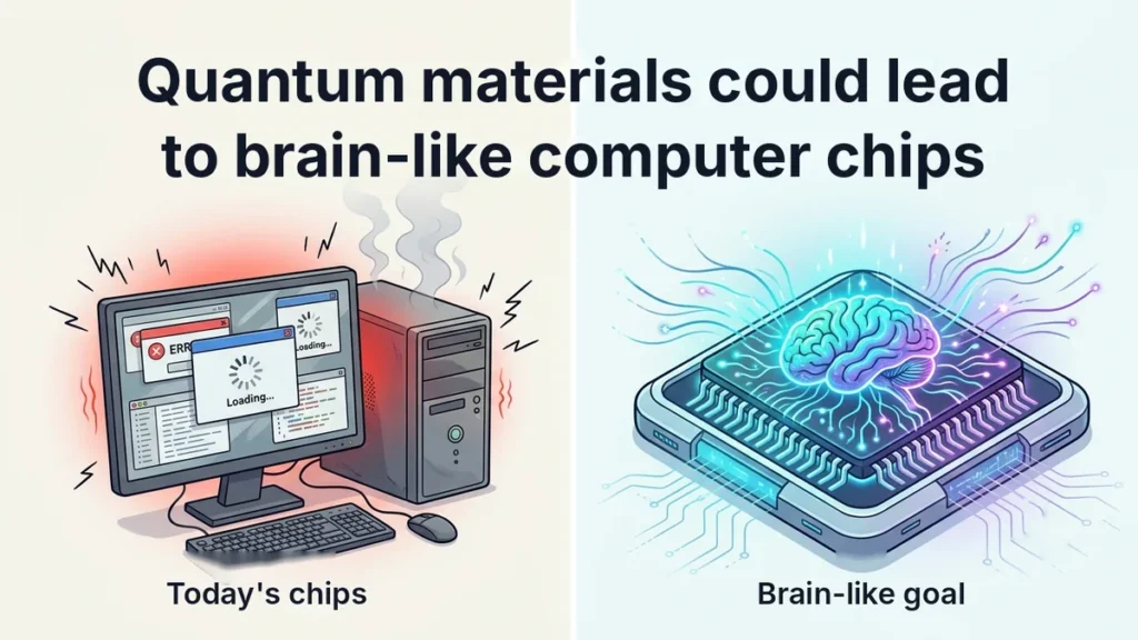
Most computers shuttle data back and forth between memory chips and processors. Every trip costs time and energy, and the trips add up quickly. Engineers have squeezed amazing gains from silicon for decades, but progress keeps getting harder. Meanwhile, your brain stores and processes information in the same place. UC San Diego physicists note that the brain runs on roughly a light bulb’s worth of power. That gap explains the growing interest in neuromorphic, or brain-like, hardware. Such chips would mix memory and processing, much like neurons and synapses do. Ordinary silicon switches don’t naturally keep a trace of what just happened. Certain quantum materials do, and that’s what makes them so tempting. The catch is simple to state but hard to solve. Nobody fully understands how that memory forms inside these materials.
Fig. 1: From Power-Hungry Computers Toward Brain-Like Chips
Why Some Materials Hold a Memory
Think about a sponge after you squeeze it under water. It doesn’t spring back right away, so it keeps a “memory” of the squeeze. Some quantum materials behave in a loosely similar way. Argonne’s feature focuses on complex oxides, compounds of metals and oxygen. They can flip between conducting and insulating, or between magnetic and nonmagnetic states. Temperature, strain, or electric and magnetic fields can trigger those flips. Here’s the interesting part: the effect can linger after the trigger disappears. That leftover response acts as a simple form of memory. Researchers think it could help with tasks like pattern recognition and data analysis. Tiny defects, such as missing oxygen atoms, appear to drive these changes. To design better devices, engineers must watch those defects move as it happens.
Explainer: How X-Ray Photon Correlation Spectroscopy Works
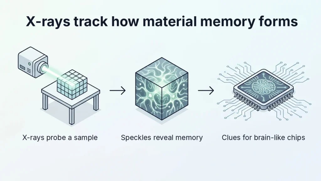
Shine a laser pointer at a rough wall, and you’ll see grainy, sparkly dots. Those dots are called a speckle pattern, and they come from coherent light. Coherent light has waves that march in step, like a well-drilled band. When such light scatters off a rough surface, the waves add and cancel unevenly. X-ray photon correlation spectroscopy, or XPCS, uses the same idea with X-rays. A coherent X-ray beam scatters off a sample and creates a speckle pattern. If atoms or defects inside the sample shift, the speckles shift too. Argonne’s Suresh Narayanan explains that tracking these changes reveals activity down to the atomic scale. Instead of one snapshot, XPCS records a movie of fluctuations. It works across timescales from millionths of a second to many minutes. That range matters, because memory effects can unfold slowly or very fast.
Fig. 2: How XPCS Tracks Memory Forming and Fading
Why Brighter, More Coherent X-Rays Matter
Speckle methods need lots of coherent X-rays, and coherent light was once scarce. Argonne’s recent upgrade changed that situation quite a bit. The Advanced Photon Source now makes beams up to 500 times brighter than before. Argonne calls it the brightest synchrotron X-ray source in the world. The upgrade also raised the share of coherent X-rays in each beam. More coherence means sharper speckles and better views of small variations. Tighter focusing helps too, so scientists can study crystals only a few micrometers wide. In the past, many experiments needed large, nearly perfect crystals instead. Higher-energy X-rays now pass through heaters, coolers and pressure cells around a sample. As a result, researchers can watch materials while they are heated, squeezed or magnetized. That’s how real devices actually live and work.
Inside Argonne’s X-Ray Look at Material Memory
The XPCS work happens at beamline 8-ID of the Advanced Photon Source. Argonne physicist Yue Cao, who uses the beamline, points out that quantum materials aren’t uniform. They vary from one tiny region to the next, and they change over time. XPCS helps link those local wobbles to big properties like conductivity and magnetism. For brain-like devices, the key question is how memory builds up and then fades. XPCS can “track how memory in these materials forms and fades over time,” says Argonne physicist Zahir Islam. That insight is valuable for quantum materials engineering, because design needs cause and effect. If engineers know which defects hold memory, they can tune growth recipes. They might add or remove defects on purpose, a bit like seasoning food. Today’s feature describes capabilities and ongoing work, not one finished experiment.
Other Beamlines Chasing Quantum Behavior
XPCS is only one of several tools in Argonne’s story. At beamline 28-ID, a newer setup watches silicon carbide grow layer by layer. Silicon carbide could host qubits, the basic units of quantum computers. Its atoms can stack in several patterns, and only some suit qubits well. The team wants growth recipes that factories could scale up later. At beamline 4-ID, scientists study materials near absolute zero or under crushing pressure. Samples squeezed between diamond tips can pass one million atmospheres. In an Oak Ridge-led study there, researchers mapped twisting magnetic patterns called chiral states. Those patterns could flip with temperature unless strain locked them in place. Antonino Miceli’s group also builds superconducting detectors that sense tiny heat changes. Together, these tools give engineers a far more complete view of quantum materials.
Why Neuromorphic Computing Matters to Chipmakers
For chipmakers, the prize is lower energy per calculation. Memory that lives inside the switching material could cut constant data shuffling. That would challenge the standard design where memory and processors sit apart. Research centers are already chasing this goal with public funding. In fact, the US Department of Energy backs the Q-MEEN-C research center led by UC San Diego. Since 2018, it has worked on quantum materials for brain-inspired, energy-efficient hardware. The department later renewed its support with $12.6 million in fresh funding. Its partners include UC Davis, UC Santa Barbara and New York University. Labs worldwide are also testing memristors, which act like adjustable artificial synapses. ENTECH has covered a self-learning memristor chip from KAIST, for example. X-ray tools like XPCS help explain why such devices behave the way they do. Better explanations, in turn, lead to better designs and fewer failed prototypes.
A Realistic Timeline for Neuromorphic Computing
Don’t expect a brain-like laptop next year, though. Most quantum-material devices still live in research labs. Engineers must make them reliable, uniform and cheap enough to manufacture. They also need software and circuit designs that suit memory-rich hardware. A realistic horizon for wider use is roughly three to ten years. However, some simpler memristor products may arrive sooner in sensors or edge devices. Still, the path depends on understanding the materials first. That’s where facilities like the Advanced Photon Source come in. Argonne says more than 5,000 researchers use it every year. Teams usually apply for beam time through a competitive proposal process. Thus, anyone in quantum materials engineering will likely use such facilities at some point. For a broader look at the field, read our review of where brain-inspired chips are heading.
Future Careers in Quantum Materials Engineering
Work like this sits where physics, materials science and electrical engineering meet. Materials scientists study how structure and defects shape a material’s behavior. Engineers on the materials side then turn those findings into repeatable factory processes. Device engineers build and test the actual chips and circuits. Beamline scientists run X-ray instruments and help visiting teams plan experiments. Data scientists matter too, since XPCS produces huge streams of speckle images. The O*NET profile for materials scientists lists typical tasks and skills. Its materials engineers profile shows the manufacturing side of the work. You won’t find “quantum materials engineer” as an official job title yet. However, research groups and chip companies increasingly hire people with this exact mix of skills. Quantum materials engineering is where many of those hires will land.
How Students Can Prepare
Start with strong physics and chemistry, especially atomic structure and electricity. Calculus and linear algebra will help when you meet waves and quantum ideas. In college, pair physics with materials science or electrical engineering courses. Look for classes on solid-state physics, crystallography and semiconductor devices. Learn Python too, because modern experiments create far more data than anyone can read by hand. Summer research programs at universities and national labs offer real lab experience. Argonne’s Matthew Highland notes that facility staff support users who aren’t X-ray experts. So you don’t need to master every instrument before your first experiment. Curiosity and careful note-taking go a long way at first. You can even try a simple speckle demo at home with a laser pointer and a wall. Just never point the laser at anyone’s eyes. Safety habits matter in every lab, from home to Argonne.
Limits Worth Keeping in Mind
This news describes tools and research directions, not a finished product. Argonne’s feature doesn’t report a specific new device or efficiency number. Memory effects in complex oxides are still being mapped and debated. Defects that help one property can hurt another, such as reliability. Scaling lab materials into billions of identical chip elements is extremely hard. XPCS also needs a large synchrotron, so factories can’t use it on production lines. Its main role is to guide design choices earlier in development. Even so, watching memory form and fade gives engineers clues they never had. For students, that makes quantum materials engineering an exciting field to watch and maybe join. Who knows, your future job might start with a speckle pattern. Stranger things have launched great careers in science.
U.S. Department of Energy Office of Science. (n.d.). Quantum Materials for Energy Efficient Neuromorphic Computing (Q-MEEN-C). Energy Frontier Research Centers. https://sc.osti.gov/bes/efrc/Centers/QMEENC
The piece explains a demanding X-ray technique in plain language and connects it sensibly to brain-inspired computing. It should be clear to readers that the source is a laboratory feature about facility capabilities, not a report of a single new experiment. The link between material memory and future chips is presented as a research goal, which is appropriate. Readers who want the full description of each instrument should check the original source article this story draws on.
Editorial note
ENTECH is running this story because brain-inspired computer chips could change how much energy computing uses, and understanding the materials behind them comes first. It gives students a clear example of how X-ray science connects physics, materials science and chip design. It also points to growing careers that blend laboratory research with hardware engineering. The article describes research tools and directions rather than a finished device, so practical chips are still some way off. For the full details, we suggest readers turn to the original article from the laboratory behind this story.
Hrutanshu Kurankar is a Computer Engineering graduate from Marathwada Mitra Mandal’s College of Engineering, Pune. His interests span artificial intelligence, machine learning, cybersecurity, data science, and science communication. He enjoys exploring how emerging technologies work and translating complex technical concepts into clear, accessible explanations for students and young audiences.
His practical experience includes developing FlashCTI, a Retrieval-Augmented Generation (RAG) system for cyber threat intelligence and log analysis, exploring privacy-focused browser extensions, and building machine learning applications. His technical background includes Python, data analysis, machine learning frameworks, web development, vector databases, and cybersecurity tools. Through these projects, he has developed an interest in applying technology to real-world problems and making technical knowledge easier to understand.
Hrutanshu is associated with ENTECH STEM Magazine, where he contributes to science communication and editorial initiatives, including research outreach and activities supporting the Machine Learning Special Issue 2026. His work involves connecting with potential contributors and academic reviewers to encourage participation in STEM research and knowledge sharing. As a science communicator, he aims to bridge the gap between complex scientific ideas and everyday understanding through relatable examples, clear writing, and evidence-based explanations. He is particularly interested in making science and technology engaging and accessible to the next generation of learners.