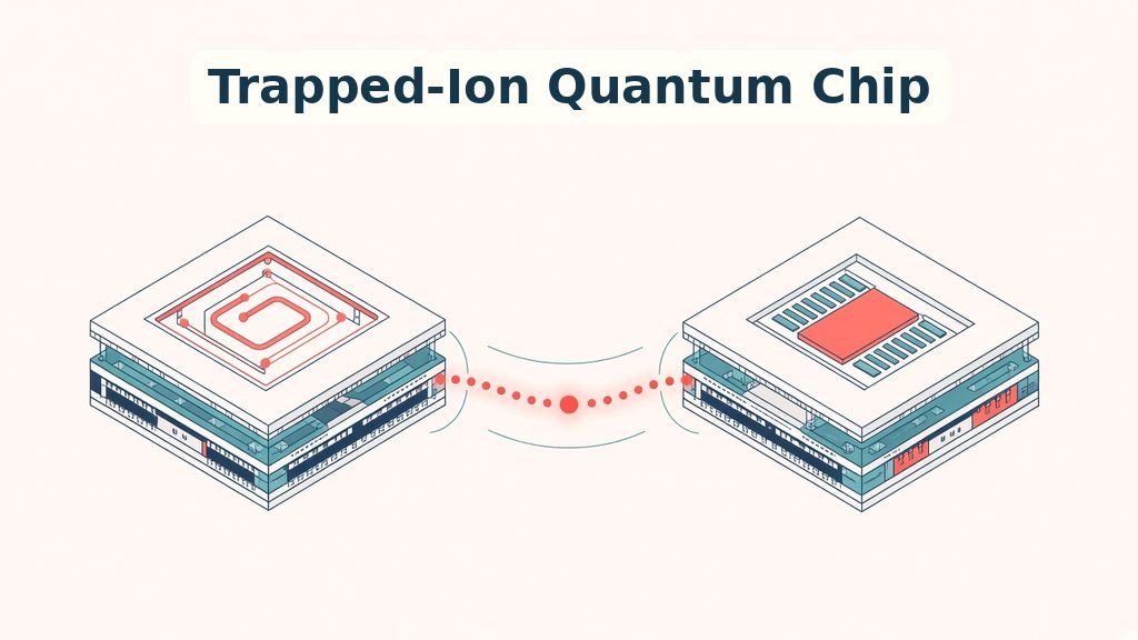
A school computer needs more than a processor to run its programs. Its circuits must also deliver power, carry signals, and connect distinct parts. Similarly, quantum hardware faces a fierce test beyond making single qubits work. A qubit is a unit that stores quantum information. On November 3, 2026, Universal Quantum announced its trapped-ion quantum chip, the iQPU which stands for integrated quantum processing unit. Its design combines not only an ion trap but also control circuits. It also includes interfaces planned to connect separate chips into larger machines. However, an assembled part does not establish a useful, large quantum computer. The official announcement describes a hardware approach, rather than a finished computing breakthrough. In contrast to that ambition, client integration and bigger builds remain future steps. Thus, for students, the central story concerns how engineers join these pieces together.
Why A Trapped-Ion Quantum Chip Needs A Scaling Plan
Building more qubits can force engineers to rebuild the machine around them. Universal Quantum identifies that repeated redesign as a central scaling challenge. Meanwhile, signals must still reach the right places without overwhelming the hardware. On the one hand, adding qubits can expand the planned computing system. In contrast to that growth, separate controls can multiply the supporting equipment. So, the firm combines parts that otherwise demand links outside the chip. Its official announcement calls this challenge the wiring problem. However, reducing external links does not remove the need for precise control. The design must address both needs inside the same small assembly. As a result of this, integration becomes more than a packaging choice. Instead, it becomes part of the plan for building a larger machine. That tension drives the iQPU design, as the dated company release explains.
The Wiring Challenge Extends Beyond A Bigger Surface
A larger trap surface alone cannot solve every barrier the team describes. Control, manufacturing, and module links must also fit the wider system plan. Therefore, the release groups those needs instead of treating them as separate upgrades. Engineers must not only hold ions but also move them across the trap. They also need circuits that direct those movements through the chip. Meanwhile, a growing system needs a way to connect more computing space. The iQPU places these roles inside a repeatable engineered unit. However, the release supplies no full system resource comparison against competing machines. Readers should distinguish the stated design purpose from a measured overall saving. In contrast to that missing comparison, the design itself has a clear purpose. It aims to prevent every expansion from demanding a wholly distinct machine. ENTECH’s ion-trap fabrication report explores another route toward building quantum hardware.
A Modular Ion Processor Needs Repeatable Boundaries
Universal Quantum describes the iQPU as a unit engineers can make again. Mike Newman, the firm’s engineering vice president, explains that planned repeatability. Indeed, he describes how the unit can be “manufactured, tested and connected repeatedly.” In other words, the boundary around each module matters alongside its inner workings. Rather than redesigning everything, engineers aim to extend the same basic design. However, the firm’s timeline still labels multiple-module iQPU assembly as upcoming. That distinction separates an assembled building block from its planned larger arrangement. Likewise, interfaces inside a module do not establish every future system layout. The linked technical page reports an assembled first iQPU. In contrast to that completed assembly, client delivery remains an upcoming milestone there. As a result, these statements show progress while leaving the largest hardware test ahead. The next challenge involves repeating the unit without losing control across its boundaries.
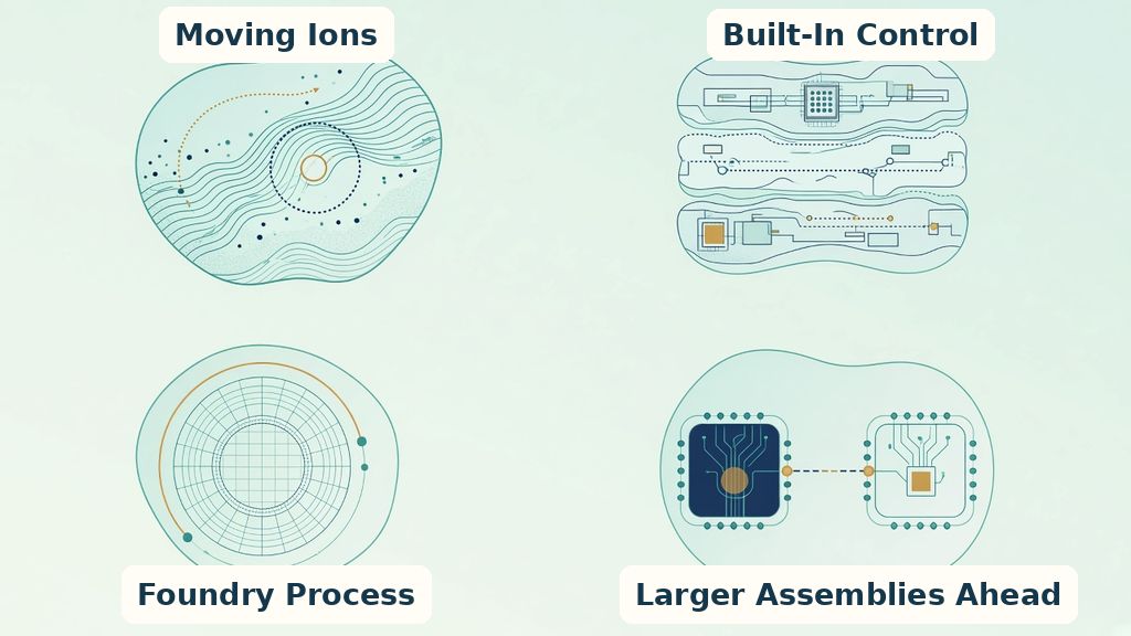
Fig. 1: Building Blocks And Remaining Milestones
Inside The Trapped-Ion Quantum Chip: A Plain-Language Explainer
This design uses trapped ions, charged atoms that serve as carriers of quantum data. Its trap gives a surface across which the system can move those ions. First, picture separate work areas connected by controlled routes across a chip. In contrast to fixed locations, moving ions lets the design change qubit links. As a result of this, distant areas need not remain isolated from each other. Indeed, the release names this arrangement a Quantum Charge-Coupled Device, or QCCD. Here, the useful idea concerns moving information carriers between distinct working zones. However, the routes do not make the chip an ordinary electronic processor. They belong to a design that controls ions for quantum operations. In other words, the movement supports computing rather than simply rearranging stored parts. Also, the team links this freedom with error correction, which tackles mistakes. Those are design aims, not evidence that every target application already works.
How An Integrated Ion Processor Routes Control Signals
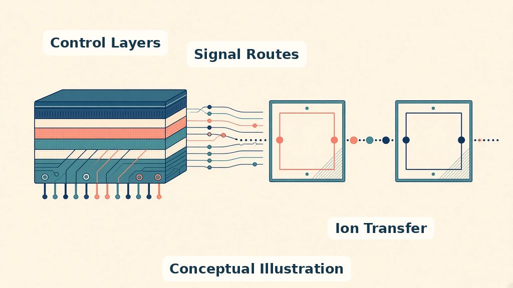
The linked technical page separates the assembly into layers with distinct jobs. An ion-trap layer gives the surface where the ions move. Next, routing layers distribute control signals through the chip. Control signals travel not only sideways but also through the chip’s silicon. Next, vertical links carry those signals between distinct layers of the assembly. Indeed, engineers call those links through-silicon vias, or TSVs for short. A simple comparison is a building with corridors and vertical service shafts. Meanwhile, a custom circuits layer handles switching and control inside the assembly. The page calls this layer an ASIC, meaning an application-specific integrated circuit. As a result of this arrangement, signals need not crowd every outside edge. Thus, the sides stay available for neighboring modules, according to the team. The diagram explains planned roles rather than giving a full manufacturing blueprint. ENTECH’s chip-based sensing report discusses a distinct integration problem.
Moving Ions Between Neighboring Modules
A connection between chips must do more than fasten their packages together. Universal Quantum calls its modular connection method UQConnect. Indeed, the design page says neighboring modules have precisely aligned trap surfaces. In other words, the pathway continues across a boundary between separate chips. As a result of this alignment, trapped-ion qubits can move between the modules. Thus, the firm describes that transfer as the basis for operating a larger computer. This differs from merely placing independent chips beside each other on a shelf. However, the iQPU timeline still leaves multi-module assembly as upcoming. Reported interconnect performance does not remove that remaining assembly step. In contrast to single part claims, a large assembly must link the whole system. Therefore, the distinction between connection technology and completed deployment deserves careful attention. The design offers a route toward expansion, not proof of unlimited expansion today.
Fig. 2: Control Layers Meet Module Links
Making The Module: Foundries, Control, And Cold Hardware
Manufacturing gives another hard boundary between a lab concept and a repeatable part. The release says the iQPU uses a commercial semiconductor foundry line. Indeed, that line handles wafers measuring two hundred millimeters across. In other words, its circular starting wafers span twenty centimeters in diameter. Rather than inventing every factory step, the approach uses established industry tools. However, the design page also specifies a modified process design kit. That kit contains the rules engineers follow when designing for the chipmaking process. So, a commercial line does not mean an entirely unchanged factory recipe. The source frames repeated production and testing as reasons for choosing this route. In contrast to that production aim, neither page publishes manufacturing yield figures. Moreover, the pages provide no measured production costs for readers to compare. The hardware argument concerns a fit with existing tools, not a demonstrated price advantage.
Surface Area Is Not A Qubit Count
Its dated release lists an active compute area exceeding four hundred square millimeters. That means more than four square centimeters of working surface. Indeed, four square centimeters equals a square two centimeters on each side. On the other hand, a qubit count measures these carriers, not physical area. In other words, readers cannot turn surface size directly into computing capacity. However, the linked page lists four hundred square millimeters, without the extra qualifier. Here, the dated release supplies the wording used for the active area. Meanwhile, the design page describes control hardware operating at seventy kelvin. That is roughly a quarter of typical room temperature on the absolute scale. As a result of that comparison, the cooling claim becomes easier to place. However, that hardware spec does not state the ions’ precise motional temperature. ENTECH’s optical-control chip report examines a distinct hardware route.
What The Announcement Establishes—And What Comes Next
The linked timeline reports a first iQPU assembly joining trap, control, and interface. It also reports earlier work on stacked circuits and a working trap prototype. However, those milestones do not establish a completed fault-tolerant quantum computer. In other words, assembling the pieces differs from proving useful computing that resists errors. On the other hand, client delivery remains upcoming despite the assembly milestone. Indeed, the dated announcement says client systems will integrate the iQPU. It names the German Aerospace Center, DLR, among those clients. Meanwhile, DLR’s planned uses include mission planning, climate modeling, and materials design. The release presents those subjects as research goals, not reported computing outcomes. As a result of this distinction, the next milestones deserve separate attention. Therefore, integration, repeated operation, and practical tasks represent distinct tests of this approach. The dramatic shift lies in packaging the scaling problem, not declaring it finished.
Performance Claims Need A Clear Testing Context
Universal Quantum’s linked page states test figures for operations and modular links. For example, it lists two-qubit gate fidelity at ninety-nine point nine percent. Put simply, that benchmark is near perfect, but still short of perfect. On the other hand, the page gives no detailed testing protocol. In other words, readers lack the conditions needed for a full technical comparison. Therefore, this article treats it as a company spec, not an independent test result. Neither captured page links an iQPU research paper or a downloadable technical spec. Likewise, neither gives a full client-system benchmark showing a useful advantage. These omissions limit what the release alone can establish about performance. As a result of this, part progress must remain separate from claims of use. Next, useful evidence would connect full assemblies with clearly described tests. That would help readers assess use rather than relying on design descriptions alone.
Conclusion: Follow The Engineering Beyond The First Assembly
The iQPU story centers on bringing several hardware problems inside a repeatable unit. Universal Quantum combines ion trapping, integrated control, and interfaces for neighboring chips. However, the official timeline still leaves delivery and bigger builds ahead. Rather than a finished story of useful computing, this release describes a hardware foundation. In other words, the next chapter depends on what engineers build with it. Therefore, the design illustrates links between physics and electronic engineering for STEM students. Ion control, silicon routing, and assembly each add to the same system. Meanwhile, the sources do not count future hiring or job displacement. Career readers should avoid treating the release as a labor-market forecast. As a result of this hardware focus, the lesson stays practical rather than promotional. Thus, a trapped-ion quantum chip needs working parts and a credible scaling path. The real test comes when those parts operate together beyond the first assembly.
The strongest thread is the connection between chip design and system growth. Keep the boundary between an assembled module and a working larger machine visible. A brief note on test conditions would help readers interpret the company’s performance claims. Readers can explore the technical context in Universal Quantum’s original official announcement.
Editorial note
This Innovation-track explainer follows a company announcement and its linked processor page, not a peer-reviewed iQPU study. It separates reported assembly milestones from proposed customer uses and future multi-module systems. Conceptual illustrations show design ideas rather than exact device layouts. For the developer’s own account, consult the original official announcement.
Aditya Joshi is an SDE Intern at Coneixement India, the company behind ENTECH STEM Magazine and STEMQuiz. He is a Computer Engineering graduate from Savitribai Phule Pune University (SPPU), with honours in Machine Learning and Data Science. His academic background and hands-on project experience have developed his interest in artificial intelligence, emerging technologies, software development, and the practical applications of computing.
His areas of technical interest include Artificial Intelligence (AI), Generative AI, Machine Learning, Data Science, Large Language Models (LLMs), Natural Language Processing (NLP), Retrieval-Augmented Generation (RAG), GraphRAG, and knowledge graphs. Through projects involving locally hosted language models, Neo4j knowledge graphs, multilingual chatbots, and AI-powered analytics, he has explored how emerging technologies can be used to solve practical problems.
Aditya's professional experience includes work in frontend development, AI/ML application development, and full-stack software projects. During his internships at Maharashtra Knowledge Corporation Limited (MKCL) and Hilwitz Solutions, he worked on applications involving web technologies, Python, Flask, and AI-driven functionality. He has also developed projects such as SalesCope, an AI-assisted sales analytics platform, and a multilingual chatbot designed to help users explore Indian government schemes.
At ENTECH STEM Magazine and STEMQuiz, Aditya brings a technology-focused perspective shaped by his engineering education and practical experience with AI and software systems. He is interested in making complex science and technology concepts easier to understand through clear explanations, relatable everyday examples, and an emphasis on how emerging innovations work and affect real-world applications.
His broader goal is to help bridge the gap between technical concepts and public understanding, encouraging curiosity about artificial intelligence, computing, and the technologies shaping the future.