Quantum Motion and partners turned a thin film already inside a commercial 22-nm silicon chip into a superinductor, making a charge sensor about 10,000 times smaller than usual designs.
Every phone in a classroom carries a chip with billions of tiny switches. Factories print those switches by the trillion, cheaply and reliably. Quantum computers, however, still lean on bulky parts that do not shrink easily. Now a new study offers a hopeful fix: a CMOS chip superinductor. Thomas Swift, Fernando Gonzalez-Zalba, and John Morton of Quantum Motion led the work. Partners came from University College London, Imperial College London, and CIC nanoGUNE in Spain. The University of Cambridge and IKERBASQUE also joined the team. Their paper appeared in Nature Electronics on November 4, 2026. For readers who want the source, the DOI is 10.1038/s41928-026-01728-8. In short, the team built a sensitive part from a layer factories already make. As a result, a key quantum sensor became dramatically smaller.
The headline result is all about size. Normally, this kind of sensor needs a coiled part called a spiral inductor. On a chip, that coil is large enough to spot by eye. In contrast, the new superinductor fits in a strip 0.36 micrometers wide. Its length of 50 micrometers roughly matches the width of a thin hair. As a result of this, it packs about 10,000 times more inductance per area. On top of that, the finished sensor works remarkably fast. It picked up a clear signal in just four billionths of a second. Still, one point needs care from the start. The team tested the device as a charge sensor, which detects single electrons. However, it has not yet read the state of a real qubit. Even so, the result marks an exciting step toward mass-produced quantum chips.
A quantum computer stores information in qubits, which follow the strange rules of quantum physics. One popular type traps single electrons inside silicon. These spin qubits measure only a few billionths of a meter across. Because they are so small, engineers hope to pack millions onto one chip. Reading each qubit, though, requires a sensor that notices tiny electrical changes. ENTECH has covered related efforts, such as an atom-thin quantum light chip. For spin qubits, the favorite sensor is a radio-frequency single-electron transistor. To put it simply, one extra electron changes how this switch behaves. Unfortunately, that sensor needs a large partner part. As a result of this, the readout hardware dwarfs the qubits it serves. In the long run, that mismatch limits how many qubits fit on a chip.
What a CMOS Chip Superinductor Replaces
The partner part is an inductor, a component that resists sudden changes in current. Most chips build inductors as flat metal spirals. According to the paper, those spirals store 50 to 200 nanohenries per square millimeter. That sounds technical, but the meaning stays simple: spirals hog space. In contrast to that, a superinductor offers very high opposition to fast-changing signals. Scientists call this opposition impedance, and it works like resistance for alternating current. A superinductor’s impedance tops a natural benchmark of about 6,450 ohms. Until now, builders made superinductors from special parts such as Josephson junctions. A Josephson junction joins two superconductors with a thin barrier between them. Others used superconducting nanowires or twisted sheets only atoms thick. For this reason, each option demands custom steps that ordinary chip factories skip.
How the CMOS Chip Superinductor Was Built and Tested
CMOS stands for complementary metal-oxide-semiconductor, the standard recipe behind nearly every computer chip. The team used a commercial 22-nanometer process from GlobalFoundries. Inside that recipe sits a very thin film of titanium nitride. Engineers normally treat this film as part of a resistor, not a special device. At extremely low temperatures, however, the film turns superconducting. According to the Nature Electronics study, one version switched near 0.75 kelvin. The other switched near 1.1 kelvin, roughly one degree above absolute zero. Next, the researchers measured how much inductance the film provides. They found about 7 to 8 nanohenries per square micrometer. In other words, the film beats typical chip spirals about 10,000 times over. Finally, they placed the film in a tuned circuit beside a tiny silicon island.
Results From the Superinductor Charge Sensor
That island acts as a quantum dot, a trap holding electrons one at a time. Together with the superinductor, it formed a complete charge sensor on one chip. Then the team cooled the chip to about 10 millikelvin. That is just one hundredth of a degree above absolute zero. After that, they measured how clearly the sensor separated two charge states. In four billionths of a second, the signal power beat the noise 4,500 times. From those data, they estimated a benchmark time of about one trillionth of a second. At that benchmark, signal and noise become equal. By contrast, the previous best value sat near 625 trillionths of a second. In other words, the new sensor reached that benchmark hundreds of times sooner. Above all, the whole sensor fit in a tiny footprint of only 18 square micrometers.
Fig. 1: Key Results From The Superinductor Charge Sensor
Explainer: How Inductors and Cold Films Sense Single Electrons
Think of an inductor as an electrical flywheel. Once current flows, the inductor resists quick changes, like a heavy spinning wheel. Ordinary inductors get this effect from magnetic fields around coiled wire. A superconductor, by contrast, carries current with zero resistance below a critical temperature. Inside it, electrons travel in linked pairs called Cooper pairs. Those pairs carry momentum, so they resist sudden changes in speed. This extra effect, called kinetic inductance, adds inertia without any coil at all. Very thin films show the effect most strongly. In this way, a flat strip can behave like a big coil while staying tiny. ENTECH readers may recall similar cold superconducting circuits research on quantum refrigeration. Engineers then pair the inductor with a capacitor to form a tuned circuit. Such a circuit rings at one frequency, like a tuned guitar string.
Why the Integrated Superinductor Boosts Sensitivity
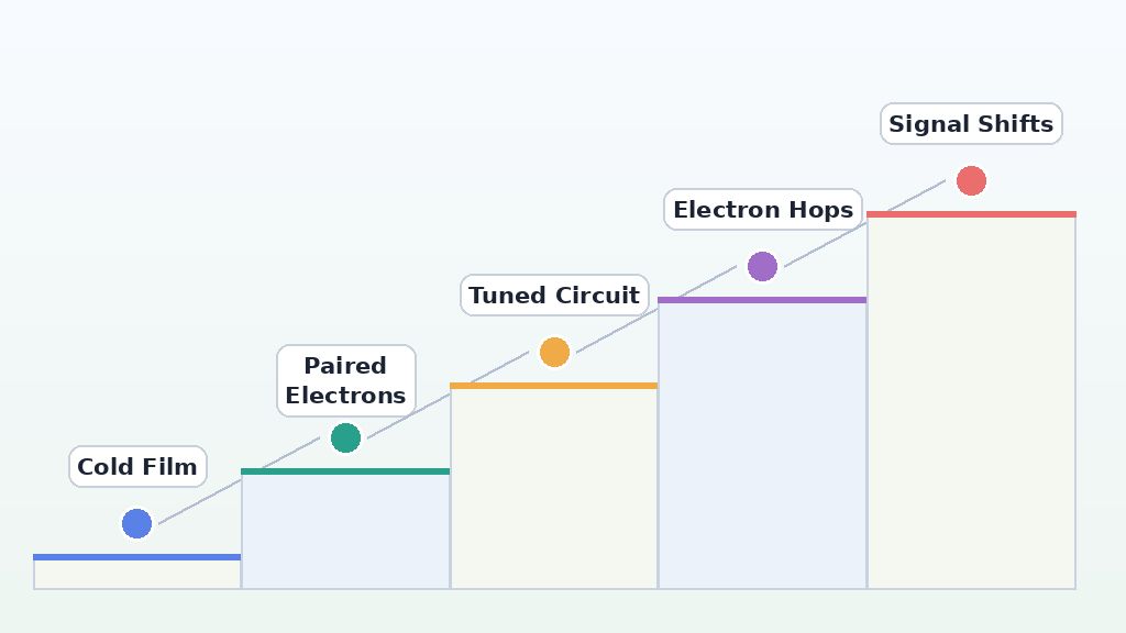
The tuned circuit links to the single-electron transistor beside it. When one electron hops onto the island, the transistor’s resistance changes. As a result, the circuit reflects a slightly different radio signal to the instruments. Scientists read that change to learn whether the electron moved. Here, the titanium nitride film added a bonus. At stronger signal levels, its inductance shifted slightly with the current itself. Instead of hurting the sensor, this nonlinear behavior amplified the reflected signal change. The researchers also built a model that predicted this extra boost. Notably, the model’s turning point matched the measured turning point very closely. Beyond that point, the wait for a clear signal dropped much faster with power. In practice, though, pushing power too high makes the film stop superconducting. So the integrated superinductor works best inside a sweet spot of signal strength.
Fig. 2: How A Cold Film Senses One Electron
Challenges and Motivation Behind the CMOS Chip Superinductor
The motivation behind the CMOS chip superinductor comes from a scaling headache. Useful quantum computers may need around a million qubits. Each qubit needs readout, and each readout circuit needs space, power, and wiring. Because of this, bulky spiral coils make that goal hard to reach. The Quantum Motion news release notes that people can spot a spiral by eye. Building the solution posed real challenges too. On the one hand, outsiders cannot easily check the film’s thickness inside the factory recipe. Yet, on the other hand, the team needed reliable numbers to design circuits. For this reason, they assumed a typical thickness of about three nanometers. They then measured many strips of different widths and lengths. In addition, they handled slight warming from the chip’s own electronics.
What the Researchers Say About Scaling
Lead author Tom Swift sees the bigger picture clearly. In his view, the field talks about scalability but focuses mainly on qubits. “We need to think about the scalability of the entire system,” Swift said. For this reason, he wants readout and control parts to shrink toward qubit size. Fernando González-Zalba, Quantum Motion’s vice president of quantum engineering, shares that optimism. “We’ve created a method with a compact on-chip footprint,” González-Zalba said. He described the method as “extremely sensitive” while staying low in power. Beyond the company, González-Zalba leads quantum hardware research at CIC nanoGUNE. Importantly, both quotes describe goals and design strengths, not finished qubit readout. At the same time, both researchers work at the company behind the chip. Their enthusiasm therefore reflects a company view alongside the paper’s data.
Limits: A Charge Sensor, Not Qubit Readout Yet
The study shows a strong charge sensor, but it does not read qubits yet. To read a spin qubit, engineers first convert its spin into a charge change. This experiment skipped that step and measured charge directly. So the paper names high-fidelity spin readout as the next goal. For that step, the team plans to use multigate transistors. Also, the chip must sit inside a dilution refrigerator near absolute zero. That makes it a lab result rather than a ready product. Similarly, the trillionth-of-a-second figure comes from extending measured trends. In addition, one author holds a related patent, as the paper discloses. Several authors also work at Quantum Motion. None of this cancels the progress, though. Instead, it shows where the next experiments must deliver with real qubits.
Conclusion: Where On-Chip Superinductors Could Go Next
This study shows that a CMOS chip superinductor can grow from an ordinary factory layer. Not only did the strip shrink a key sensor, but it also sped it up. That combination gives silicon quantum computing a welcome, practical boost. Beyond qubits, the authors see uses in radio astronomy and faint-light detectors. They also suggest compact amplifiers and smaller cold electronics. Partner institute CIC nanoGUNE highlights the same broad possibilities. For students, the work links circuit design, materials science, and quantum physics. As a result, careers in chip design and cryogenic testing may grow alongside it. In the same way, quantum hardware roles could expand as factories adopt such parts. Next, the team must prove the integrated superinductor reads real spin qubits reliably. Until then, this bright result stands as a superb sensor demonstration.
References
Swift, T. H., Gomez-Saiz, A., Olivieri, F., Aizpurua-Iraola, G., Suárez-Rodríguez, M., Kirkman, J., Noah, G. M., de Kruijf, M., von Horstig, F.-E., Morton, J. J. L., & Gonzalez-Zalba, M. F. (2026). A nonlinear superinductor in a deep-submicrometre integrated circuit. Nature Electronics. https://doi.org/10.1038/s41928-026-01728-8
Swarali keeps the tone upbeat while still flagging that this is a sensor demonstration rather than working qubit readout, which is the right balance. The explainer could add a simple sketch-style comparison between an ordinary coil and the thin film so younger readers picture kinetic inductance faster. A sentence on why the chip must stay so cold, and what that means for real machines, would also help. Readers are encouraged to go to the original source paper in Nature Electronics for the full methods and data.
Editorial note
A note from the editors: we wrote this piece at our simpler reading level, so some technical detail from the paper has been trimmed or rounded into plain comparisons. We invite readers to check the specifics for themselves in the original research paper that this story draws from.
Swarali Barpande is an Electronics and Telecommunication Engineer and technology enthusiast based in Pune, India. She is passionate about making complex physics and engineering concepts accessible, with a core focus on applied electromagnetics, signal transmission, and fundamental circuit theory.
As an author for ENTECH Magazine, Swarali specializes in breaking down foundational topics such as electromagnetism, electromagnetic induction, and modern telecommunication principles for students and young STEM researchers. Through her writing, she aims to bridge academic engineering fundamentals with real-world technological applications.