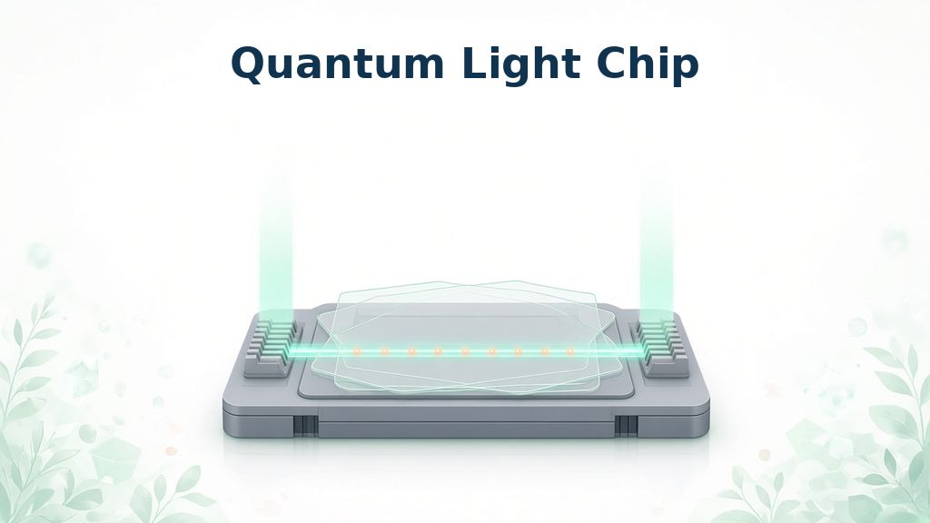
Every phone photo uses a sensor that catches billions of light particles at once. Quantum computers need the opposite, namely one particle of light at a time. A Danish team has now built a quantum light chip from atom-thin crystals. Pietro Metuh led the study as first author. Battulga Munkhbat supervised the work at the Technical University of Denmark, known as DTU. In particular, the team works in Electrical and Photonics Engineering and the NanoPhoton center. At the same time, they placed tiny light emitters directly on top of light-carrying channels. As a result, single photons flowed straight into the chip with very high purity. The paper appeared on October 28, 2026, in Nature Communications (DOI: 10.1038/s41467-026-78806-0). For now, however, the chip works only near minus 269 °C, about 4 kelvin. Even so, it marks a clear early step for chip-based quantum light.
The Science Explained: How a Quantum Light Chip Works
Light-based quantum computers and networks need three parts on one chip. First, a source must emit single photons, one at a time. Next, waveguides must steer those photons like tiny optical wires. Finally, detectors must count each photon at the end. Today, however, each part usually needs its own material and process. Circuits often use silicon or silicon nitride, for example, while emitters use other semiconductors. Detectors, in turn, rely on special superconductors such as NbTiN or MoSi. ENTECH Magazine explains the bigger picture in its guide to optical quantum computing. Because of this mix, joining parts needs complex hybrid fabrication with strict heat limits. According to the authors, this mismatch has become a major bottleneck for scaling up. For this reason, the DTU team tested whether one layered family could do every job. Their answer came from crystals only a few atoms thick.
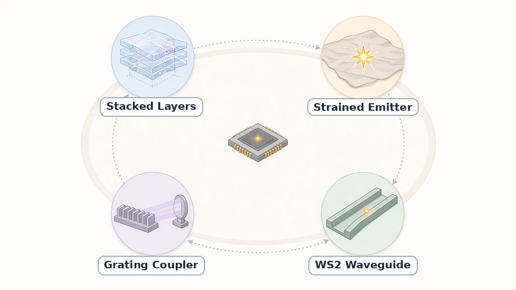
Fig. 1: How a Quantum Light Chip Works
Single Photons and Why Purity Matters
A single-photon source should never release two photons at the same moment. Scientists test this with a number called g2(0), the second-order correlation at zero delay. A perfect source scores 0, while a weak laser beam scores 1. To measure it, researchers split the light toward two detectors. If both detectors never click together, the source emits photons one by one. This classic test is the Hanbury Brown and Twiss setup. In short, lower values mean purer single photons. Purity matters because quantum protocols treat each photon as a separate carrier of information. Two photons at once, by contrast, can spoil a calculation or a secure message. For this reason, chip builders want values close to 0. In addition, they want high brightness so that many photons reach the circuit. Overall, a useful source must be both pure and bright.
Stacking Atom-Thin Layers Like Sticky Notes
The chip uses van der Waals materials, crystals that peel into atom-thin sheets. These sheets stick to almost any flat surface, much like sticky notes on a desk. First, the team shaped tungsten disulfide, or WS2, into waveguides 500 by 150 nanometers. Next, they added grating couplers with a 780-nanometer pitch at each end. These ridged patterns let light leave the chip toward a lens. Then they laid hexagonal boron nitride, under 5 nanometers thick, on the waveguide. Finally, they placed a two-layer sheet of tungsten diselenide, or WSe2, on top. Small strains in that sheet, for example wrinkles, create quantum emitters. Similar thin WSe2 sheets first emitted single photons a decade ago (Tonndorf et al., 2015). Because the team simply transfers each layer, the process needs no vapor deposition. In other words, the method can add emitters to existing photonic circuits.
Challenges and Motivation Behind 2D Quantum Photonics
Layered crystals called transition metal dichalcogenides, or TMDs, have drawn wide interest in photonics. Some host quantum emitters, while others guide light or even detect single photons. NbSe2 nanowires, for instance, have already detected single photons (Zugliani et al., 2026). On paper, then, one material family could cover the whole circuit. In practice, however, nobody had built a complete chip from these layers. The U.S. National Quantum Initiative treats such quantum hardware as a research priority. Boron nitride, in the meantime, can form light-trapping cavities (Kim et al., 2018). A single material platform, in principle, could cut fabrication steps and compatibility problems. Earlier emitters also performed poorly once they sat on top of waveguides. As a result, the field still lacked a bright, pure and integrated 2D light source. That gap set the main research goal for the DTU team.
Why Earlier Layered Emitters Fell Short
The key problem is coupling efficiency, meaning how much emitted light enters the waveguide. In hexagonal boron nitride, emitters form inside the waveguide itself, so coupling comes naturally. TMD emitters, by contrast, need strain, so engineers must transfer a separate sheet on top. That sheet is only one or two layers thick. Because of this, it cannot reshape the light traveling below. Earlier designs also targeted the waveguide’s basic light pattern, called the fundamental mode. Light in that mode overlaps only weakly with emitters sitting on the surface. Past layered emitters scored g2(0) of 0.15 to 0.69 (Peyskens et al., 2019). Their waveguide-coupled photon rates also stayed below one million per second. In contrast, the DTU team took a different route. They used a thicker multimode waveguide carrying several light patterns. Some patterns overlap better with the emitter, so more photons enter the chip.
Key Findings From the Quantum Light Chip Study
To start, the team cooled the chip to about 4 kelvin inside a cryostat. Then they scanned a laser along the waveguide to find emitters. One bright emitter, called QE1 in the paper, glowed at 802 nanometers. The team compared two ways to excite it. Above-band excitation used a 650-nanometer laser, while discrete-state excitation used 783 nanometers. The second method pumped the emitter more gently, just above its own energy level. As a result, emission grew roughly ten times brighter at equal laser power. At the same time, the emitter’s decay time dropped from 55.0 to 31.1 nanoseconds. In addition, the light stayed strongly polarized, near 84% at the coupler. Several emitters within the same flake coupled to the waveguide as well. Notably, bilayers placed without the boron nitride layer cracked and coupled more weakly. For this reason, the thin spacer proved essential.
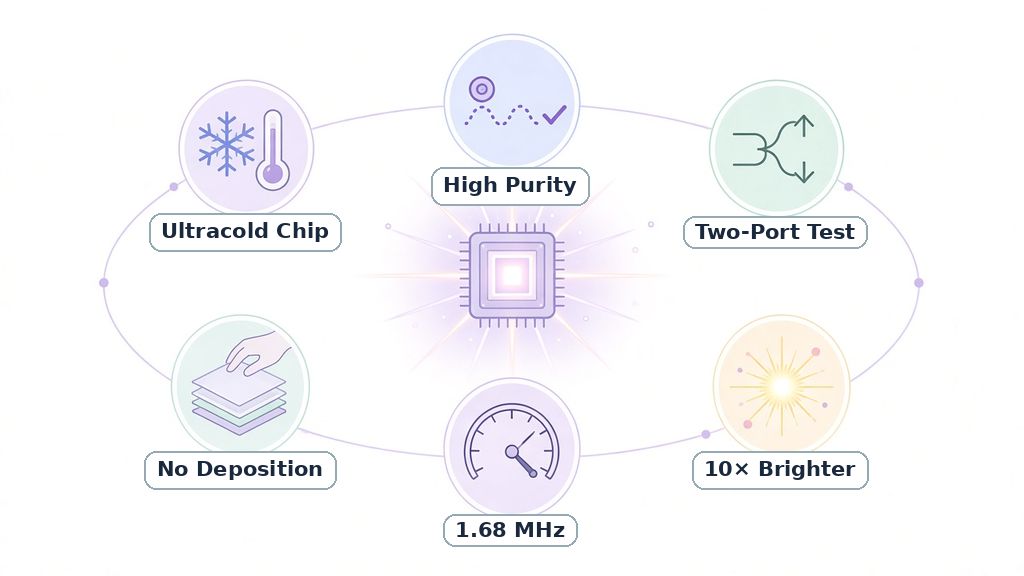
Fig. 2: Key Numbers From the Quantum Light Study
Single-Photon Purity on the Quantum Light Chip
Next, the team measured purity in three setups. With a lens directly above the emitter, g2(0) reached 0.043. Collecting light through a grating coupler gave an even lower value of 0.003. In fact, its uncertainty of up to 0.030 puts it near the error limit. Then the team tried a smarter trick. Because the waveguide has two ends, they correlated photons leaving both ports. This setup made the usual external beam splitter unnecessary. The waveguide itself now split the photon stream. It still gave a low g2(0) of 0.076, with an uncertainty of 0.023. According to the authors, two separate ports make the test more robust than one. All three setups therefore confirmed high single-photon purity. However, the traces also showed blinking, so the brightness flickered at times. Such flicker remains a known issue for this class of emitter.
Brightness and Photon Count Rates
Brightness matters as much as purity for practical chips. Brighter sources feed more photons into each circuit. At the detectors, the team counted 20.0 and 14.5 thousand photons per second. After setup losses, that equals about 357 and 259 thousand per second at the lens. The grating couplers, however, release only part of the light. Simulations put their best-case efficiency at 21.2%, with an average of 12.2% across modes. Using that upper limit, the team estimated at least 1.68 million waveguide-coupled photons per second. The opposite direction carried at least 1.22 million per second. In fact, the authors call these conservative estimates, because real couplers likely perform below simulations. Overall waveguide brightness, which includes every single loss, stayed at 0.65% or more. Even so, these megahertz-level rates top earlier layered emitters on waveguides. In short, the multimode design clearly improved coupling.
Business Opportunities and Careers in Quantum Photonics
Right now, photonics labs and component makers can test 2D emitters on existing circuits. Within about five years, prototype chip-based sources might serve quantum communication and sensing. That outcome depends on whether purity, brightness and yield hold up. Beyond five years, entire circuits might combine sources, waveguides and detectors from 2D materials. Still, several serious technical limits stand in the way. The chip works only near 4 kelvin, so it needs a bulky cryostat. Its detectors also sat off the chip, as superconducting nanowire detectors in the lab. The authors have not yet measured indistinguishability, a key property for many quantum protocols. They also want shorter decay times, steadier emission and systematic studies of transfer yield. Electrical biasing and high-quality optical cavities could, according to the paper, improve brightness further. For this reason, the work remains an early lab demonstration.
Quantum Light Chip Careers and Study Paths
This research blends physics, engineering and materials science, so it opens several career paths. Quantum photonics engineers design circuits that create, route and detect single photons. Nanofabrication and cleanroom engineers pattern waveguides and transfer atom-thin flakes with care. Optical physicists, in turn, run cryogenic tests such as photon correlation measurements. Materials scientists who study 2D crystals search for brighter and steadier emitters. To prepare, students can study physics with a focus on quantum optics. Electrical and photonics engineering also fits well, as well as materials science or nanotechnology. Lab skills with lasers, cryostats and microscopes matter in every one of these roles. ENTECH Magazine covered related work on low-loss quantum photonic chips that steer visible light. In addition, a new chip setup for quantum networks shows where such sources could fit. Strong math and coding skills help with simulation work too.
Conclusion
This quantum light chip shows that atom-thin crystals can both make and guide single photons. A bilayer WSe2 sheet created the emitters, while WS2 waveguides carried their light. In addition, a thin boron nitride spacer protected the sheet and boosted brightness. As a result, photons entered the waveguide with g2(0) values as low as 0.003. The chip also reached estimated waveguide-coupled rates of at least 1.68 million photons per second. However, it works only near 4 kelvin, and its detectors still sit off the chip. Indistinguishability and transfer yield, in fact, still need testing. Even so, the study offers a clear path toward circuits built mostly from 2D materials. For students, it links quantum optics with nanofabrication. Full details appear in the open-access paper by Metuh and colleagues in Nature Communications. Future work on detectors, cavities and indistinguishability will decide its reach.
References
Kim, S., Fröch, J. E., Christian, J., Straw, M., Bishop, J., Totonjian, D., Watanabe, K., Taniguchi, T., Toth, M., & Aharonovich, I. (2018). Photonic crystal cavities from hexagonal boron nitride. Nature Communications, 9, Article 2623. https://doi.org/10.1038/s41467-018-05117-4
Metuh, P., Wyborski, P., Paralikis, A., Schröder, F., Stenger, N., Gregersen, N., & Munkhbat, B. (2026). Integrated on-chip quantum light sources on a van der Waals platform. Nature Communications. Advance online publication. https://doi.org/10.1038/s41467-026-78806-0
National Quantum Initiative. (n.d.). About the National Quantum Initiative. Retrieved November 2, 2026, from https://www.quantum.gov/about/
Peyskens, F., Chakraborty, C., Muneeb, M., Van Thourhout, D., & Englund, D. (2019). Integration of single photon emitters in 2D layered materials with a silicon nitride photonic chip. Nature Communications, 10, Article 4435. https://doi.org/10.1038/s41467-019-12421-0
Tonndorf, P., Schmidt, R., Schneider, R., Kern, J., Buscema, M., Steele, G. A., Castellanos-Gomez, A., van der Zant, H. S. J., Michaelis de Vasconcellos, S., & Bratschitsch, R. (2015). Single-photon emission from localized excitons in an atomically thin semiconductor. Optica, 2(4), 347. https://doi.org/10.1364/OPTICA.2.000347
Zugliani, L., Palermo, A., Scaparra, B., Patra, A., Wietschorke, F., Metuh, P., Paralikis, A., De Fazio, D., Kastl, C., Flaschmann, R., Munkhbat, B., Müller, K., Finley, J. J., & Barbone, M. (2026). Single-photon detection in few-layer NbSe2 superconducting nanowires. Nature Communications, 17, Article 7586. https://doi.org/10.1038/s41467-026-75646-w
Reviewer's comment
The single-photon purity claim rests on two measurement setups, one port and a cross-correlation between two waveguide ports, which makes it more robust than a single measurement. The brief accurately reports the purity values, the 357 kHz count rate, and the 1.68 MHz estimated waveguide-coupled rate, and it correctly labels the 1.68 MHz figure as an estimate. It also states the 4 K operation and the authors' own open problems. Readers should know that the detectors were not on the chip; photons left through grating couplers and were measured with off-chip superconducting detectors, and the paper lists on-chip detection as a future milestone. The correlation traces also show some blinking. No correction needed; the brief's wording stays within the paper's results.
Editorial Note
Quantum computers and secure light-based networks need single-photon sources on the same chip as the circuits that carry the photons. We are running this story because a Technical University of Denmark team stacked atom-thin crystals, WSe2 emitters on WS2 waveguides, and showed high-purity single photons traveling through the chip. The layers can be placed on existing photonic circuits, which could simplify manufacturing later. Caveats: the device works at about 4 K, and photon indistinguishability has not yet been measured. Takeaway: quantum hardware is still early, so students who learn optics and nanofabrication now will be ready as the industry grows.
Mahi Shitut is a Science Communicator at ENTECH STEM Magazine, with a BSc in Physics from Fergusson College, Pune, and an ongoing MSc in Mathematics at the Indian Institute of Science Education and Research (IISER), Kolkata. Her areas of interest include theoretical physics, pure mathematics, astronomy, space science, set theory, asymptotic series, and science education. She completed the National Initiative in Undergraduate Science (NIUS) Physics Programme at the Homi Bhabha Centre for Science Education, TIFR, Mumbai, where she carried out a 1.5-year research project at the UM-DAE Centre for Excellence in Basic Sciences. She was also a top scorer in the Madhava Mathematics Competition and was selected for the Madhava Nurture Camp at IIT Bombay, and she attended the IWM Winter School for Young Women in Mathematics.
Mahi specializes in explaining advanced physics and mathematics in simple, clear, and easy-to-understand language for teenagers and school students. Drawing on everyday examples and practical analogies, she helps readers make sense of ideas like infinity, space missions, telescopes, and how the universe works, without losing scientific accuracy. Her skill comes from hands-on experience. She has explained models of Chandrayaan-3 to more than 3,000 visitors at IUCAA’s National Science Day open day, volunteered at SPPU’s National Space Day celebrations, presented at Fergusson College’s Astro Club Poster Exhibitions, and delivered undergraduate lectures on countability and uncountability, the infinite hotel paradox, and asymptotic series through the Synectics Math Club. With earlier experience in editorial work and content strategy, including editing a newsletter and writing for digital audiences, she aims through ENTECH STEM Magazine to bridge the gap between advanced science and public understanding, making physics and mathematics engaging, accessible, and relevant for young minds.