Sunscreen bottles warn about ultraviolet (UV) rays because that light carries lots of energy. Yet the same energetic light also powers some of science’s most precise tools. For example, ultraviolet lasers help control charged atoms inside trapped-ion quantum computers. Even so, labs still shape that light with bulky crystals and kilovolt-level drivers. In contrast, a Belgian team built ultraviolet modulator chips that work at gigahertz speeds. Chupao Lin led the work with supervisor Bart Kuyken at Ghent University–imec in Belgium. Their thin-film lithium tantalate chip has an active section only 200 micrometers long. It reached a 3-decibel bandwidth above 40 gigahertz with 375-nanometer light. The team reported the results on October 27, 2026, in Nature Communications (DOI: 10.1038/s41467-026-78862-6). As a result, compact ultraviolet circuits for clocks, sensors and quantum machines look more practical.
The Science Explained: How an Ultraviolet Modulator Chip Works
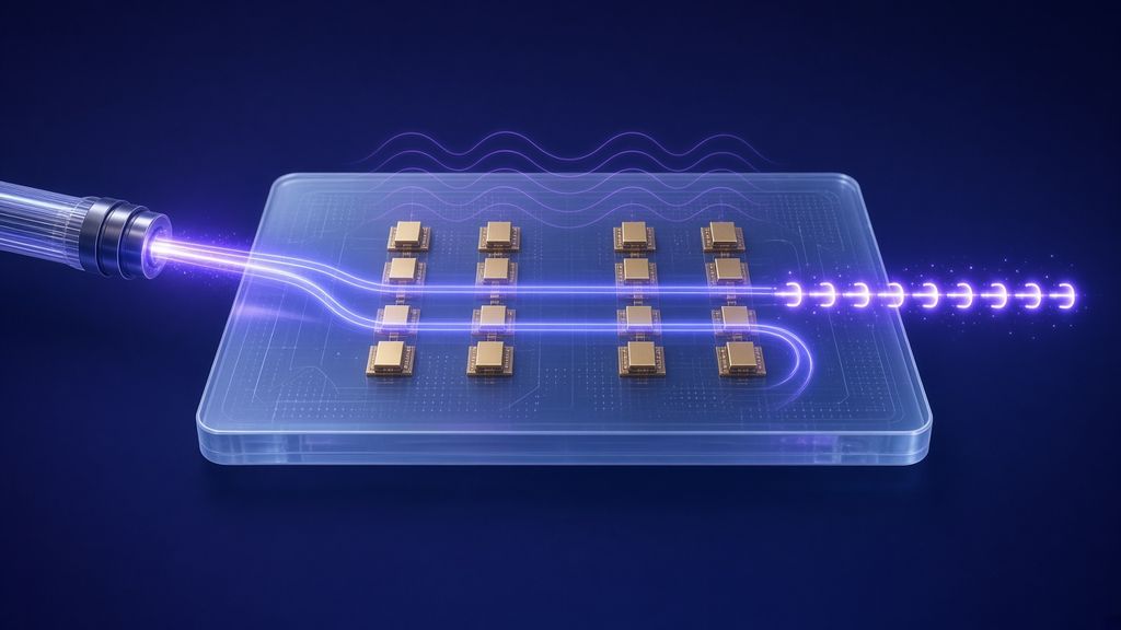
A modulator works like a very fast shutter that writes a message onto light. In this chip, light travels through a waveguide, a narrow ridge that traps it. To begin with, a splitter called a multimode interferometer divides the beam into two arms. In turn, a second splitter joins the two beams near the exit. Engineers call this layout a Mach-Zehnder interferometer, or MZI. When one beam lags slightly, the two waves add up or cancel out.
In other words, a tiny delay decides how much light leaves the chip. To create that delay, metal electrodes apply voltage across both arms at once. The field pushes the refractive index up in one arm and down in the other. Because of this opposite shift, the needed voltage drops by half. Engineers name this trick push-pull driving. Notably, the team chose an MZI over ring resonators for robustness. Unlike rings, an MZI tolerates temperature swings and small fabrication errors.
Fig. 1: How an Ultraviolet Modulator Chip Works
Why Lithium Tantalate Suits Ultraviolet Light
The chip’s key ingredient is lithium tantalate, a crystal with a strong electro-optic effect. Such materials change their refractive index almost instantly when voltage arrives. Its cousin, lithium niobate, already leads fast modulators for telecom light. However, lithium niobate suffers from the photorefractive effect at short wavelengths. Strong blue or UV light disturbs its optics and causes instability. In contrast, lithium tantalate stays transparent down to about 275 nanometers.
It also shows a photorefractive index change about ten times smaller than lithium niobate. At the same time, its response to temperature is about ten times weaker. Earlier measurements by Juvalta and colleagues tested its electro-optic behavior at UV wavelengths. UV light brings one more bonus for modulators. Because phase shift grows as wavelength shrinks, short wavelengths magnify the effect. As a result, a 200-micrometer electrode switches the light fully at just 4.2 volts. By comparison, telecom devices need lengths about a hundred times longer.
Challenges and Motivation Behind Ultraviolet Modulator Chips
Today’s fast ultraviolet modulators still rely on large crystals such as beta-barium borate. Another common crystal, called DKDP, faces the same limits. Because their electrodes sit far apart, they need half-wave voltages of kilovolts. Driving such voltages at gigahertz rates heats the crystals badly. For this reason, their practical intensity modulation tops out at hundreds of megahertz. Chips offer a smaller, steadier choice, but UV options remain few.
For example, alumina waveguides guide UV light well yet lack an electro-optic effect. Because of this, engineers tune them with tiny heaters that work at tens of kilohertz. Heaters also leak warmth into neighboring circuits, a problem called thermal crosstalk. Recently, Castillo and colleagues tried small piezo actuators that flex alumina chips. In fact, their mechanical design reached tens of megahertz, a big step forward. Still, the actuator’s mechanical resonance capped its speed. Clearly, the field needed a chip-scale modulator that reaches gigahertz speeds with UV light.
Scattering Grows Fast at Short Wavelengths
UV light poses a tougher problem than visible or infrared light. Common chip materials like silicon and silicon nitride absorb it strongly. Due to their narrow bandgaps, UV photons vanish into the material. At the same time, Rayleigh scattering grows as one over wavelength to the fourth power. In plain terms, halving the wavelength multiplies scattering about sixteen times. Earlier lithium tantalate waveguides already lost up to 4 decibels per centimeter at 532 nanometers.
Crystal defects from wafer slicing likely absorb UV light as well. Yet the payoff for solving these problems is large. For instance, trapped ytterbium ions need phase modulation at 12.6 gigahertz near 369.5 nanometers. That frequency matches a key energy split inside the ion. Trapped-ion quantum computers depend on such precise UV control. Likewise, fast UV modulation could support wireless data links above 100 gigahertz. For that reason, the Ghent team set out to build fast UV modulation on chips.
Key Findings on Ultraviolet Modulator Chips
The team started with a commercial wafer of x-cut lithium tantalate on insulator. Its lithium tantalate layer measured just 300 nanometers thick. First of all, electron-beam lithography drew the circuit pattern into a resist layer. Next, a wet bath of citric acid, potassium hydroxide and peroxide etched the ridges. This etch reached 100 nanometers deep and left nearly vertical sidewalls. Smooth surfaces matter because roughness scatters UV light so strongly. Indeed, atomic force microscopy showed a surface roughness of only 0.2 nanometers. Waveguide width tapers from 2.7 micrometers at the facets to 0.42 micrometers inside. The team narrowed it so that only one light mode travels inside. Titanium-gold electrodes leave a gap of only 1.5 micrometers between them. The whole modulator measures 1.16 millimeters long, yet its active section spans 200 micrometers. Finally, a 375-nanometer laser fed the chip through a single-mode optical fiber.
Loss, Voltage and Speed of the Ultraviolet Modulator Chip
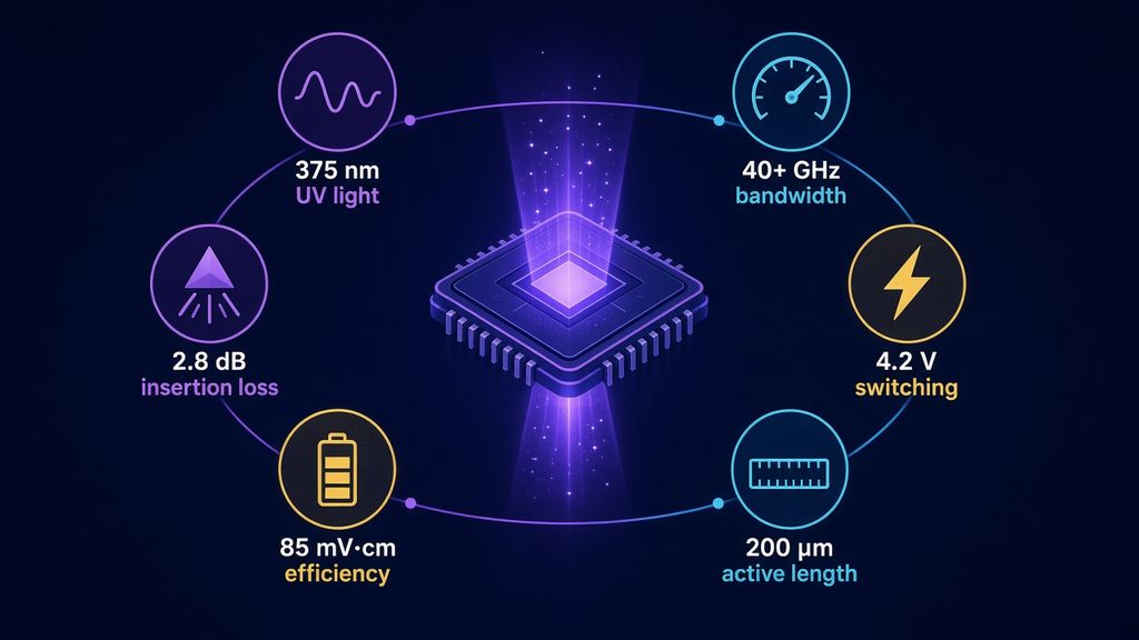
According to the paper, the waveguide lost 7.2 decibels per centimeter at 375 nanometers. That figure rises from 2.0 decibels per centimeter at 780 nanometers, as scattering predicts. Because of its short length, the device’s on-chip insertion loss stayed at 2.8 decibels. Next, the team measured the half-wave voltage, the voltage that flips the output fully. It reached 4.2 volts, a level compatible with standard CMOS chip electronics. Multiplied by length, that equals 85 millivolt-centimeters. Across six devices, the spread stayed at just 2 millivolt-centimeters. That value beats typical telecom-wavelength modulators by more than ten times. Meanwhile, the best extinction ratio reached 22.7 decibels between on and off states. Speed tests then showed a 3-decibel bandwidth above 40 gigahertz. Electrode tests up to 67 gigahertz lost only 2 decibels of microwave signal. From those tests, the team estimated just 1 decibel of optical roll-off at 67 gigahertz.
Fig. 2: Key Numbers From the UV Modulator Chip Study
Limits the Team Still Faces
Some results still leave room for improvement. In particular, coupling light from fiber into the chip cost 9.7 decibels per facet. Simulations had predicted 7.5 decibels, so the setup lost extra light. Spot-size converters, already proven on other platforms, could shrink this loss. In addition, the measured on-chip insertion loss exceeded the 1.3-decibel prediction. The authors suspect electrode misalignment and coupling variations caused that gap. Similarly, the speed test hit the limits of available equipment. Its photodetector targets near-infrared light, so UV readings may drift. On the positive side, the chip showed no photodarkening at high power. It handled an on-chip intensity of 5 kilowatts per square millimeter for five minutes. Over time, the team plans to test oxygen annealing to repair crystal defects. In addition, a silicon dioxide top layer could reduce scattering further. Notably, the chip also reached 0.12 volt-centimeters at 448 nanometers, in blue light.
Implications: Business, Careers and What to Study
For industry, the most important detail may be the starting material. The team used commercial thin-film lithium tantalate from the supplier NanoLN. Because the wafers already exist on the market, foundries could adopt the process sooner. The authors say the platform suits wafer-scale chip making. Several markets could gain from small, fast UV photonics. For example, trapped-ion quantum computers need fast, stable control of UV lasers. Portable atomic clocks could also shrink if bulky optics move onto chips.
In communications, UV light links can work without a direct line of sight. Europe is already investing in this field. The Horizon Europe QU-PIC project funded the work and targets universal quantum photonic chips. Meanwhile, imec and Ghent University have shown micro-transfer printing of lithium tantalate onto silicon photonics. Such printing could one day add tantalate modulators to low-loss alumina circuits. Still, the authors note that joining lithium tantalate to alumina remains hard.
Career Paths and What to Study
This project shows how many skills one small chip demands. Lin conceived the experiments, then designed and fabricated the device. Five team members developed the waveguide process flow together. Others measured material loss as well as the high-speed response. Accordingly, several career paths connect directly to this kind of work. Photonic integrated circuit designers lay out waveguides, splitters and electrodes. Cleanroom and nanofabrication engineers turn those layouts into real chips. Optoelectronics engineers test lasers, light sensors and fast signals. Quantum technology engineers then build these parts into larger systems. For high school students, physics and mathematics form the strongest foundation. Later, university degrees in electrical engineering, physics or materials science fit well. Courses in optics, radio-frequency design and nanotechnology add useful depth. At the same time, coding skills help with simulations like the team’s mode-matching models. Even a short internship in a university lab can show how chips take shape.
Conclusion: Ultraviolet Light Moves Onto the Chip
This study tackles a long-standing gap in UV photonics. Passive UV chips, on the one hand, already guided light with low loss. On the other hand, fast switching still required bulky crystals and high voltages. The Ghent team bridged that gap with thin-film lithium tantalate. Their 200-micrometer modulator needed only 4.2 volts and passed 40 gigahertz. By a combined speed-and-voltage measure, it beat bulk lithium niobate modulators a hundredfold. Still, coupling loss and fiber alignment need work before products appear. Next, annealing and better couplers could cut those losses further. Even so, the path from lab bench to factory now looks shorter. Similar work on tiny optical chips for quantum computing points in the same direction. For students, the message is clear: optics, materials and electronics now meet on one chip. In the end, ultraviolet modulator chips could bring precise quantum tools out of the lab.
References
Castillo, Z. A., Shugayev, R., Dominguez, D., Gehl, M., Karl, N., Leenheer, A., Little, B., Jau, Y.-Y., & Eichenfield, M. (2026). CMOS-fabricated ultraviolet light modulator using low-loss alumina piezo-optomechanical photonics. Optica Quantum, 4(2), 114–120. https://doi.org/10.1364/OPTICAQ.582412
European Commission. (n.d.). Quantum Universal Photonics Integrated Circuit platform (QU-PIC) [Project fact sheet]. CORDIS. Retrieved October 28, 2026, from https://cordis.europa.eu/project/id/101135845
Juvalta, F., Jazbinsek, M., Günter, P., & Kitamura, K. (2006). Electro-optical properties of near-stoichiometric and congruent lithium tantalate at ultraviolet wavelengths. Journal of the Optical Society of America B, 23(2), 276–281. https://doi.org/10.1364/JOSAB.23.000276
Lin, C., Nenezic, P., Moerman, A., Cammarata, S., Atzeni, S., Akritidis, K., Vanackere, T., Niels, M., Li, H., Bonito Oliva, V., Yin, X., Billet, M., & Kuyken, B. (2026). Thin-film lithium tantalate for ultraviolet integrated electro-optic modulator. Nature Communications. Advance online publication. https://doi.org/10.1038/s41467-026-78862-6
The device data are consistent: the half-wave voltage-length product of 85 mV·cm varied by only 2 mV·cm across six modulators, and the 7.2 dB/cm waveguide loss at 375 nm is measured with care. The article reports the main numbers accurately. Readers should know that "above 40 GHz" reflects a 40 GHz RF probe and a photodetector calibrated for near-infrared light, so the true bandwidth is not known; the 1 dB roll-off at 67 GHz is an estimate from electrode tests. The 2.8 dB loss is on-chip only, and each fiber connection cost another 9.7 dB. Photodarkening was checked for five minutes, and patterning used electron-beam lithography. Fix: the paper reports about a hundredfold lower VπL than bulk crystals, not a combined speed-and-voltage measure.
I am a Physics graduate with a strong academic interest in statistical mechanics, complex systems, computational physics, and the study of collective behaviour in interacting systems. During my undergraduate studies, I developed an interest in understanding physical phenomena not only through theoretical concepts but also through computational modelling and simulation. As part of my academic work, I explored the Ising model using Monte Carlo simulations and studied the Active Ising Model to investigate collective behaviour, density variations, and phase transitions in active systems. These projects introduced me to computational approaches in physics and strengthened my interest in understanding how simple microscopic interactions can give rise to complex macroscopic behaviour. Alongside my academic interests, I am passionate about education and science communication. I have experience helping students and peers understand concepts in physics and mathematics, with an emphasis on intuitive explanations rather than simply memorising formulas. I enjoy connecting scientific ideas to everyday experiences and presenting complex topics in a way that is clear, engaging, and accessible. I am also interested in the role of technology in education and the development of digital learning resources. Through writing, teaching, and educational projects, I hope to contribute to making scientific knowledge more accessible to students and curious learners. My broader interests include non-equilibrium statistical mechanics, active matter, phase transitions, computational modelling, complex systems, and science education. Through my work, I aim to continue developing as a researcher while contributing to science communication and education.